Supercharge Your Innovation With Domain-Expert AI Agents!

Gate-constrained silicon-controlled rectifier and manufacturing method thereof

A silicon-controlled rectifier and gate technology, which is used in semiconductor/solid-state device manufacturing, electric solid-state devices, semiconductor devices, etc. The effect of a large design window

Pending Publication Date: 2021-12-14
SHANGHAI HUALI MICROELECTRONICS CORP
View PDF0 Cites 0 Cited by
  • Summary
  • Abstract
  • Description
  • Claims
  • Application Information

AI Technical Summary

Problems solved by technology

[0005] The problem in the prior art is that the critical dimension A / B of the gate-constrained silicon controlled rectifier has a small design window, which makes it difficult to control the critical dimension in actual manufacturing.

Method used


Image

  • Gate-constrained silicon-controlled rectifier and manufacturing method thereof
  • Gate-constrained silicon-controlled rectifier and manufacturing method thereof
  • Gate-constrained silicon-controlled rectifier and manufacturing method thereof

Examples


Embodiment Construction

[0135] A preferred embodiment of the present invention will be described in detail below in conjunction with the accompanying drawings. It should be understood that the present invention is not limited to the specific embodiments described above, and the devices and structures that are not described in detail should be understood to be implemented in a common manner in the art; Within the scope of the technical solution of the invention, many possible changes and modifications can be made to the technical solution of the present invention by using the methods and technical content disclosed above, or be modified into equivalent embodiments with equivalent changes, which does not affect the essence of the present invention.

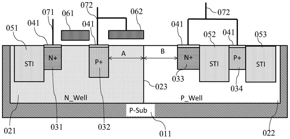
[0136] The descriptions "left", "right", "upper" and "lower" represent relative positions in the figure and should not be limited. The reference to "upper" is the opposite of what is generally defined as "lower" to describe a semiconductor substrate.

[0...


PUM

PropertyMeasurementUnit
electrical resistanceaaaaaaaaaa

Abstract

A gate-constrained silicon-controlled rectifier includes: a semiconductor substrate; an N well and a P well which are generated in the semiconductor substrate, wherein the N well and the P well are arranged adjacently, a first high-concentration P-type dopant is inserted into the P well at the interface of the N well and the P well, and the first high-concentration P-type dopant extends into the N well. Therefore, the design window of the physical critical dimension of the gate constraint silicon controlled rectifier is enlarged, the process control difficulty in practical application is reduced, and the method can be suitable for the anti-static protection design of an advanced CMOS process integrated circuit. The invention discloses a manufacturing method of a gate-constrained silicon-controlled rectifier. The method comprises the following steps: providing a semiconductor substrate; forming an N well and a P well in the semiconductor substrate, wherein the N well and the P well are arranged adjacently, a first high-concentration P-type dopant is inserted into the P well at the interface of the N well and the P well, and the first high-concentration P-type dopant extends into the N well. Therefore, the gate-constrained silicon-controlled rectifier with a large critical dimension design window can be manufactured.

Description

technical field [0001] The invention relates to the technical field of semiconductor integrated circuit devices, in particular to a gate-confined silicon-controlled rectifier. [0002] The invention also relates to the technical field of semiconductor device manufacturing, in particular to a manufacturing method of a gate-confined silicon-controlled rectifier. Background technique [0003] In the field of integrated circuit anti-static protection (ESD, Electro-Static Discharge) design, the anti-static protection design window generally depends on the operating voltage and the thickness of the gate oxide layer of the internal protected circuit. The 55-nanometer low-power (55LP) process platform is the For example, the operating voltage of the core device (1.2V MOSFET) is 1.2V, and the thickness of the gate oxide layer is 26 angstroms (Å), so the anti-static protection design window of the core device (1.2V MOSFET) of the 55nm low-power process platform is usually It is betwe...

Claims


Application Information

Patent Timeline
Patent Type & Authority Applications(China)
IPC IPC(8): H01L29/06H01L29/745H01L27/02H01L21/332
CPCH01L29/745H01L29/0684H01L29/66363H01L29/66393H01L27/0262H01L27/0296
Inventor 朱天志黄冠群陈昊瑜邵华
Owner SHANGHAI HUALI MICROELECTRONICS CORP
Features
  • R&D
  • Intellectual Property
  • Life Sciences
  • Materials
  • Tech Scout
  • Unparalleled Data Quality
  • Higher Quality Content
  • 60% Fewer Hallucinations
Learn More