Pixel structure of thin film transistor liquid crystal display and manufacturing method thereof

A technology for liquid crystal displays and thin film transistors, applied in semiconductor/solid-state device manufacturing, transistors, electric solid-state devices, etc., can solve problems such as affecting display effect, a-Si fault, image flicker or gray level change, etc., to reduce masking. The number of film exposures, the effect of simplifying the production process and reducing the overlap width

Active Publication Date: 2012-08-22
BOE TECH GRP CO LTD +1
View PDF4 Cites 5 Cited by
  • Summary
  • Abstract
  • Description
  • Claims
  • Application Information

AI Technical Summary

Problems solved by technology

[0005] Whether it is a 5Mask process or a 4Mask process, the etching requirements for the ohmic contact layer in the channel area are relatively high. If the etching is not enough, the ohmic contact layer cannot be cut off, resulting in poor contact. Excessive etching will cause a-Si faults, and the process control is difficult.
Secondly, a-Si is a light-sensitive material. In the bottom-gate structure, the conductive channel is located on the uppermost layer of the TFT. Therefore, during the use of TFT-LCD, the external light is easy to shine on the a-Si at the position of the conductive channel. In terms of materials, it affects the retention characteristics of TFT-LCD, and severe image flicker or gray level changes will occur
In addition, in order to prevent light leakage, the black matrix on the color filter glass substrate needs to have a certain overlap with the pixel electrode area of ​​the TFT on the array glass substrate. However, this overlap reduces the aperture ratio of the TFT-LCD and affects the display effect.

Method used


Image

  • Pixel structure of thin film transistor liquid crystal display and manufacturing method thereof
  • Pixel structure of thin film transistor liquid crystal display and manufacturing method thereof
  • Pixel structure of thin film transistor liquid crystal display and manufacturing method thereof

Examples


Embodiment Construction

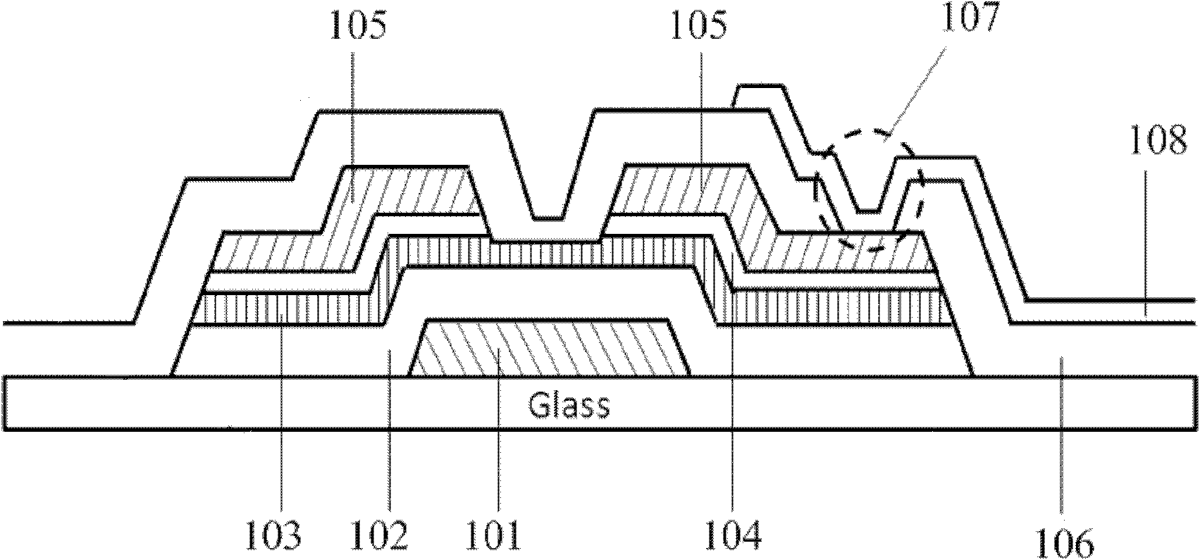
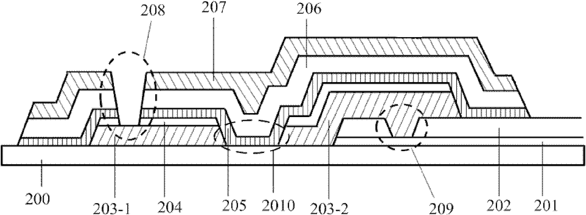
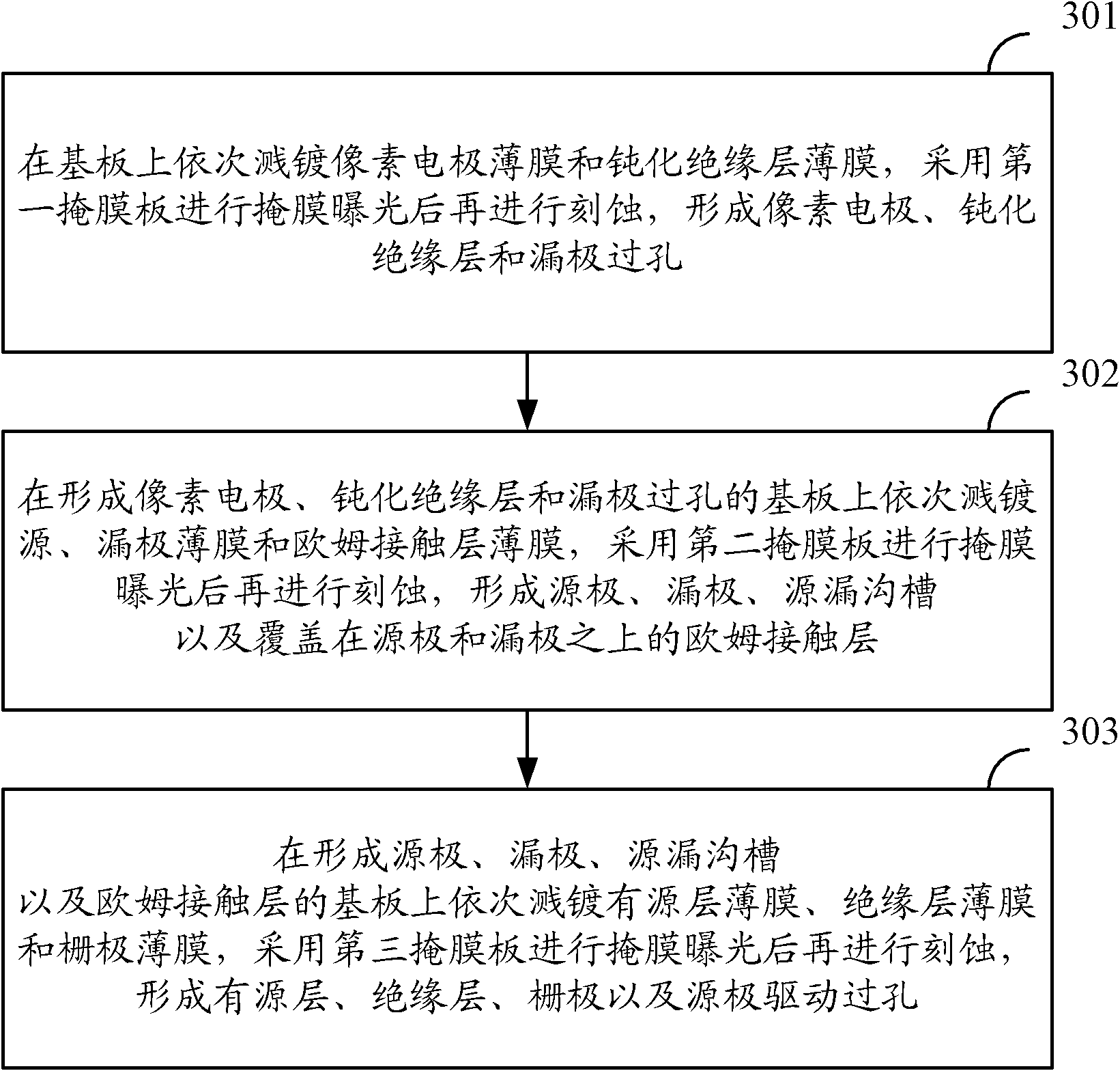
[0025] In order to reduce the number of mask exposures, simplify the production process, save costs, effectively reduce the irradiation of external light on the active layer (a-Si), improve the product yield, protect the conductive channel, and increase the TFT-LCD. The aperture ratio improves the display effect. The embodiment of the present invention provides a pixel structure of a thin film transistor liquid crystal display and a manufacturing method thereof. The method comprises: sequentially sputtering a pixel electrode thin film and a passivation insulating layer thin film on a substrate, using a first mask plate for mask exposure, and then etching to form a pixel electrode, a passivation insulating layer and a drain via hole; On the substrate where the pixel electrode, passivation insulating layer and drain via hole are formed, the source, drain film and ohmic contact layer film are sequentially sputtered, and the second mask plate is used for mask exposure and then etch...


PUM


Abstract

The invention discloses a pixel structure of a thin film transistor liquid crystal display and a manufacturing method thereof, which aim to reduce the number of mask, simplify process flow and save cost. The method comprises the following steps of sputtering a pixel electrode film and a passivation insulating layer film on a substrate in sequence; performing mask exposure by using a first mask plate and then etching the first mask plate to form a pixel electrode, passivation insulating layer and drain electrode through hole; and then sputtering source, drain electrode films and an ohmic contact layer film in sequence; performing mask exposure by using a second mask plate and etching the second mask plate to form a source electrode, a drain electrode, a source-drain channel and an ohmic contact layer covering on the source electrode and the drain electrode; and then sputtering an active layer film, an insulation layer film and a grid electrode film in sequence; performing mask exposure by using a third mask plate and etching the third mask plate to form an active layer, an insulation layer, a grid electrode and a source electrode driving hole. The invention synchronously discloses the pixel structure of the thin film transistor liquid crystal display.

Description

technical field [0001] The present invention relates to the technical field of liquid crystal displays, in particular to a pixel structure of a thin film transistor liquid crystal display (TFT-LCD) and a manufacturing method thereof. Background technique [0002] In recent years, TFT-LCD has dominated the flat panel display market due to its advantages of small size, light weight, low power consumption and no radiation. The TFT-LCD display forms an array of hundreds of thousands to millions of pixels, wherein each pixel is controlled by a thin film transistor (Thin Film Transistor, TFT) to display an image. [0003] The commonly used TFT at this stage is a bottom-gate structure using a 5-time mask (5Mask) process, and its structure is shown in the attached figure 1 As shown, the specific processing process is as follows: firstly, the gate metal thin film is prepared on the array glass substrate by magnetron sputtering, the exposure process and the chemical etching process a...

Claims


Application Information

Patent Timeline
Patent Type & Authority Applications(China)
IPC IPC(8): H01L29/786H01L21/77G02F1/1362G02F1/1368H01L27/12
Inventor 耿军郑载润吴代吾王世凯訾玉宝王建伟
Owner BOE TECH GRP CO LTD
Why Eureka
Try Eureka