Low-cadmium CIGS-based thin-film solar cell and manufacturing method thereof

A solar cell and thin film technology, applied in circuits, photovoltaic power generation, electrical components, etc., can solve the problems of difficult process control and narrow process window, and achieve the effect of reducing the thickness of the CdS layer, broadening the process window, and increasing short-circuit current.

Inactive Publication Date: 2015-12-02
蔡淼鑫
View PDF4 Cites 4 Cited by
  • Summary
  • Abstract
  • Description
  • Claims
  • Application Information

AI Technical Summary

Problems solved by technology

Therefore, in fact, the thickness of the CdS layer of the current commercial CIGS battery is gene

Method used


Image

  • Low-cadmium CIGS-based thin-film solar cell and manufacturing method thereof

Examples


Embodiment 1

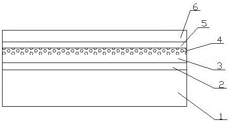
[0031] Such as figure 1 As shown, a low-cadmium CIGS-based thin-film solar cell includes a substrate 1, a back electrode 2, a CIGS absorption layer 3, a CdS layer 5, and an upper electrode 6 from bottom to top, and the Cu atoms on the surface of the CIGS absorption layer 3 are Cd atoms are partially replaced, and the thickness of the CdS layer 5 is 20 nm.

[0032] The preparation method of the low-cadmium CIGS-based thin-film solar cell includes the following steps:

[0033] a, depositing a back electrode on the substrate;

[0034] b, Depositing a CIGS absorber layer on the back electrode;

[0035] c, Depositing a CdS layer on the CIGS absorber layer;

[0036] d, depositing an upper electrode on the surface of the CdS layer;

[0037] Before the step c, modify the CIGS surface, the specific steps are: weigh CdSO 4 Powder 1.6g, dissolved in 1.276L deionized water, stirred evenly, to CdSO 4 224ml of ammonia water with a concentration of 19wt% was added to the solution, and...


PUM

PropertyMeasurementUnit
Thicknessaaaaaaaaaa
Thicknessaaaaaaaaaa

Abstract

The invention provides a low-cadmium CIGS-based thin-film solar cell and a manufacturing method thereof. The thin-film solar cell sequentially comprises a substrate, a back electrode, a CIGS absorption layer, a CdS layer and an upper electrode from the bottom up. Cu atoms on the surface of the CIGS absorption layer are partially replaced by Cd atoms to form a surface modified layer. The thickness of the CdS layer ranges from 20nm to 35nm. The manufacturing method comprises the following steps of (a) depositing the back electrode on the substrate; (b) depositing the CIGS absorption layer on the back electrode; (c) depositing the CdS layer on the CIGS absorption layer; and (d) depositing the upper electrode on the surface of the CdS layer. In the step c, an operation for modifying the surface of the CIGS surface is performed before the CdS layer is deposited. While the overall high CIGS cell conversion efficiency is kept, the thickness of the CdS layer is greatly lowered. The Cd content of a whole cell module is greatly reduced.

Description

technical field [0001] The invention relates to the technical field of thin-film solar cells, in particular to a low-cadmium CIGS-based thin-film solar cell and a preparation method thereof. Background technique [0002] Copper Indium Gallium Selenide (Cu(In,Ga)Se 2 , referred to as CIGS) thin-film solar cells have attracted widespread attention due to their high photoelectric conversion efficiency, less material consumption, light weight, and flexibility, and are considered to be the second-generation solar cells with great commercial prospects. [0003] Generally, the preparation process of CIGS thin film solar cells includes: a, depositing a back electrode on the substrate; b, depositing a CIGS absorber layer on the back electrode; c, depositing a CdS layer on the CIGS absorber layer; d, depositing a CdS layer on the surface of the CdS layer electrode. In the preparation process of CIGS thin-film solar cells, it is necessary to use a CdS layer with certain environment...

Claims


Application Information

Patent Timeline
IPC IPC(8): H01L31/068H01L31/0216H01L31/0296H01L31/032H01L31/0352H01L31/18
CPCH01L31/02168H01L31/0296H01L31/0323H01L31/03529H01L31/068H01L31/18Y02E10/541Y02E10/547Y02P70/50
Inventor 孙合成王奇于化丛
Owner 蔡淼鑫
Why Eureka
Try Eureka