Semiconductor chilling plate and manufacturing method thereof

A technology of semiconductors and refrigerating sheets, which is applied in the field of semiconductor refrigerating sheets and its production, and can solve problems such as poor anti-overload ability

Pending Publication Date: 2021-12-17
BYD CO LTD +1
View PDF8 Cites 0 Cited by
  • Summary
  • Abstract
  • Description
  • Claims
  • Application Information

AI Technical Summary

Problems solved by technology

[0005] The inventors found that the current semiconductor refrigeration chips have the problem of poor overload resistance

Method used


Image

  • Semiconductor chilling plate and manufacturing method thereof
  • Semiconductor chilling plate and manufacturing method thereof
  • Semiconductor chilling plate and manufacturing method thereof

Examples


Embodiment 1

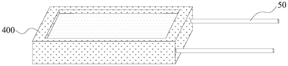
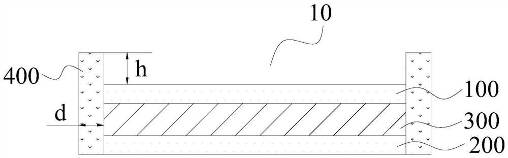
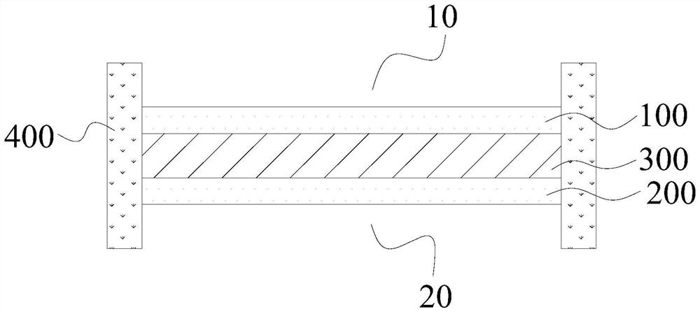
[0058] The semiconductive refrigeration sheet includes a semiconductive refrigeration assembly and a packaging structure, and the semiconductive refrigeration assembly includes a first insulating and heat conducting layer and a second insulating and heat conducting layer oppositely arranged, and a semiconductor layer located between the first insulating and heat conducting layer and the second insulating and heat conducting layer, The side of the semi-conductor refrigeration assembly provided with the first insulating and heat-conducting layer is the cold end, and the side provided with the second insulating and heat-conducting layer is the hot end. The packaging structure covers the side wall of the semiconductor refrigeration assembly and forms a second A groove, at the same time forming a second groove with the second insulating and heat-conducting layer.

[0059] Both the first insulating and heat-conducting layer and the second insulating and heat-conducting layer are cera...

Embodiment 2

[0067] The structure and manufacturing process of the semiconductor refrigeration chip of this embodiment are basically the same as that of Embodiment 1, the difference is that the wall thickness of the packaging structure is 0.8mm, the depth of the first groove and the second groove are both 0.6mm, injection molding The temperature is 240°C, the injection pressure is 40bar, and the curing time is 50s.

Embodiment 3

[0069] The structure and manufacturing process of the peltier cooler in this embodiment are basically the same as in Embodiment 1, except that the wall thickness of the packaging structure is 1 mm, and the depths of the first groove and the second groove are both 1 mm.


PUM


Abstract

The invention discloses a semiconductor chilling plate and a manufacturing method thereof. The method comprises the steps that: a semiconductor refrigeration assembly is provided, the semiconductor refrigeration assembly comprises a first insulation heat conduction layer, a second insulation heat conduction layer and a semiconductor layer, the first insulation heat conduction layer and the second insulation heat conduction layer are oppositely arranged, the semiconductor layer is located between the first insulation heat conduction layer and the second insulation heat conduction layer and comprises a plurality of couple pairs, and the couple pairs are connected in series and electrically connected with wires; and the side, provided with the first insulation heat conduction layer, of the semiconductor refrigeration assembly is a cold end, and the side, provided with the second insulation heat conduction layer, of the semiconductor refrigeration assembly is a hot end. A packaging structure is formed, the packaging structure is enabled to cover the side wall of the semiconductor refrigeration assembly, the packaging structure and the first insulation heat conduction layer form a first groove, and the wire is enabled to penetrate through the packaging structure and extend to the outer side of the packaging structure so as to obtain the semiconductor refrigeration sheet. Therefore, the obtained semiconductor chilling plate can bear the pressure of more than 1000 PSI.

Description

technical field [0001] The invention relates to the technical field of refrigeration devices, in particular to a semiconductor refrigeration chip and a manufacturing method thereof. Background technique [0002] The semiconductor refrigeration chip is a new type of refrigerator that achieves refrigeration through the Peltier effect. When direct current passes through a galvanic couple made of two different semiconductor materials in series, heat can be absorbed and released at both ends of the galvanic couple to realize refrigeration. The semiconductor refrigeration chip has the functions of refrigeration, cooling, constant temperature, etc., and can realize point-by-point temperature control, and has the advantages of small size, no mechanical transmission parts, no noise, fast cooling and heating conversion, high reliability, long life, no environmental pollution, and can be It has the advantages of miniaturization, miniaturization, reciprocity of cooling and heating. ...

Claims


Application Information

Patent Timeline
Patent Type & Authority Applications(China)
IPC IPC(8): H01L35/34H01L35/32F25B21/02
CPCF25B21/02H10N10/17H10N10/01F25B2321/023
Inventor 李永辉李俊俏周维
Owner BYD CO LTD
Why Eureka
Try Eureka