Laser debonding gas emission device and method

A gas emission and debonding technology, applied in electrical components, electric solid devices, semiconductor devices, etc., can solve the problems of pollution, easy escape of air, phase transition of bonding glue, etc.

Pending Publication Date: 2021-12-28
北京中科镭特电子有限公司
View PDF0 Cites 0 Cited by
  • Summary
  • Abstract
  • Description
  • Claims
  • Application Information

AI Technical Summary

Problems solved by technology

[0003] In the process of realizing the present invention, the inventors found that there are at least the following technical problems in the prior art: in the process of debonding the semiconductor wafer and the substrate, the phase change of the bonding glue will easily escape into the air and cause air pollution

Method used


Image

  • Laser debonding gas emission device and method
  • Laser debonding gas emission device and method
  • Laser debonding gas emission device and method

Examples


Embodiment Construction

[0038] In order to make the purpose, technical solutions and advantages of the embodiments of the present invention clearer, the technical solutions in the embodiments of the present invention will be clearly and completely described below in conjunction with the drawings in the embodiments of the present invention. Obviously, the described embodiments It is only some embodiments of the present invention, but not all embodiments. Based on the embodiments of the present invention, all other embodiments obtained by persons of ordinary skill in the art without making creative efforts belong to the protection scope of the present invention.

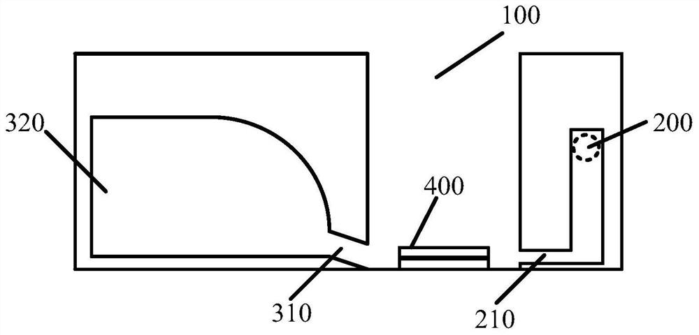
[0039] An embodiment of the present invention provides a laser debonding gas discharge device, such as figure 1 shown, including:

[0040] The debonding cavity 100 has a bearing area at the bottom, and the bearing area is used for bearing the bonding structure 400 during the debonding process;

[0041] In some embodiments, the debonding cav...


PUM


Abstract

The invention provides a laser debonding gas emission device. The device comprises: a debonding cavity, wherein the bottom of the debonding cavity is provided with a bearing area, and the bearing area is used for bearing a bonding structure in a de-bonding process; an air curtain generation module communicated with the debonding cavity through an air curtain generation opening, wherein the air curtain generation module can emit an air curtain to a bonding structure through the air curtain generation opening so as to cover the bonding structure; and a gas discharge module communicated with the debonding cavity through a discharge gas passage on a gas curtain path, so as to discharge gas of the gas curtain into the gas discharge module along the discharge gas passage. In the debonding process, the gas curtain is adopted to cover the bonding structure, and the gas emission module is adopted to carry out emission, so that gas pollution caused by phase change of the bonding glue is avoided.

Description

technical field [0001] The invention relates to the technical field of semiconductor processing, in particular to a laser debonding gas discharge device and method. Background technique [0002] In the field of semiconductor manufacturing, it is often necessary to thin the thickness of a single semiconductor wafer, so it is necessary to thin the back of a semiconductor wafer with a thickness (grinding and cutting) after loading the integrated circuit. Usually, a substrate is used to temporarily bond the semiconductor wafer (Temporary Bonding), and the substrate is used as the base of the semiconductor wafer during processing to protect the semiconductor wafer from damage due to thickness thinning during processing. After the thinning of the semiconductor wafer is completed, the semiconductor wafer and the substrate must be debonded (DeBonding). [0003] In the process of realizing the present invention, the inventors found that there are at least the following technical pro...

Claims


Application Information

Patent Timeline
Patent Type & Authority Applications(China)
IPC IPC(8): H01L21/67
CPCH01L24/799H01L21/67144H01L21/67253H01L2224/7999
Inventor 张昆鹏李纪东张紫辰侯煜张喆张彪易飞跃杨顺凯
Owner 北京中科镭特电子有限公司
Why Eureka
Try Eureka