Eureka AIR delivers breakthrough ideas for toughest innovation challenges, trusted by R&D personnel around the world.

Epitaxial reaction chamber recovery method, epitaxial growth device and epitaxial wafer

A technology of a reaction chamber and a recovery method, applied in the recovery of an epitaxial reaction chamber, epitaxial wafers, and epitaxial growth devices, can solve the problems of reduced productivity of epitaxial wafers, low MCLT value of epitaxial wafers, which cannot meet customer specifications, etc. , to achieve the effect of shortening recovery time and improving productivity

Pending Publication Date: 2022-01-11
XIAN ESWIN MATERIAL TECH CO LTD +1
View PDF5 Cites 0 Cited by
  • Summary
  • Abstract
  • Description
  • Claims
  • Application Information

AI Technical Summary

Problems solved by technology

[0004] At present, after replacing the base of the epitaxial reaction chamber, due to the adsorption of moisture and metal impurities in the new base, after the preventive maintenance (PM) of the epitaxial reaction chamber, the metal impurities in the new base still remain No removal, which leads to a high concentration of moisture and metal contaminants in the thermally stable state of the epitaxial reaction chamber at the initial recovery stage of the epitaxial reaction chamber, and the MCLT value of the produced epitaxial wafer is very low and cannot meet customer specifications
Therefore, in order to remove the moisture and metal contaminants in the thermally stable state in the epitaxial reaction chamber, it is necessary to bake and spread the epitaxial reaction chamber for a long enough time, so that the MCLT value of the epitaxial wafer obtained from the metal contamination test reach the set value, in which case the productivity of the epitaxial wafers is reduced

Method used

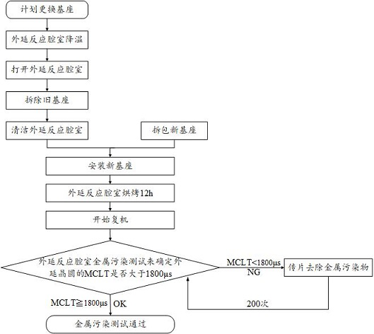

Image

  • Epitaxial reaction chamber recovery method, epitaxial growth device and epitaxial wafer
  • Epitaxial reaction chamber recovery method, epitaxial growth device and epitaxial wafer
  • Epitaxial reaction chamber recovery method, epitaxial growth device and epitaxial wafer

Examples


Embodiment Construction

[0021] The following will clearly and completely describe the technical solutions in the embodiments of the present invention with reference to the drawings in the embodiments of the present invention.

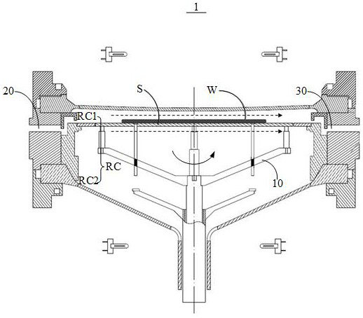
[0022] see figure 1 , which shows a schematic diagram of an existing epitaxial growth device 1 for polishing a wafer W. Such as figure 1 As shown, the epitaxial growth device 1 may include: a base S, a base support frame 10 supporting the base S, and an epitaxial reaction chamber RC, wherein the epitaxial reaction chamber RC is divided into an upper epitaxial reaction chamber RC1 and a lower epitaxial reaction chamber RC1. The reaction chamber RC2, the polished wafer W is placed in the upper epitaxial reaction chamber RC1; the gas inlet 20, the gas inlet 20 is used to transport the reaction gas in the upper epitaxial reaction chamber RC1, for example, with SiHCl 3 For example silicon source gas, hydrogen, with B 2 h 6 or pH 3 Take the dopant gas as an example, so that the...


PUM


Abstract

The embodiment of the invention discloses a recovery method of an epitaxial reaction chamber, an epitaxial growth device and an epitaxial wafer. The method includes: loading a new base into a baking chamber, and nonlinearly raising the temperature in the baking chamber according to time so as to bake the new base; after baking of the new base is completed, installing the new base in an epitaxial reaction chamber, and raising the temperature in the epitaxial reaction chamber according to set baking conditions so that the interior of the epitaxial reaction chamber can be baked; and after baking in the epitaxial reaction chamber is completed, starting to prepare an epitaxial wafer and measuring the MCLT value of the epitaxial wafer.

Description

technical field [0001] The embodiments of the present invention relate to the technical field of semiconductor preparation, and in particular to a recovery method for an epitaxial reaction chamber, an epitaxial growth device, and an epitaxial wafer. Background technique [0002] Conventional wafers are prepared through a single crystal silicon rod growth process, a slicing process, grinding engineering, a grinding process, a polishing process, and a cleaning process for removing abrasives or impurities attached to the wafer after the polishing process. Wafers prepared by this method are called polished wafers, and wafers on which a single-crystal thin film (also called an epitaxial layer) is grown on the surface of the polished wafer are called epitaxial wafers. [0003] Compared with polished wafers, epitaxial wafers have the characteristics of less surface defects, excellent crystallinity and controllable resistivity, and are widely used in highly integrated integrated cir...

Claims


Application Information

Patent Timeline
IPC IPC(8): C30B25/02C30B25/10C30B25/08
CPCC30B25/02C30B25/10C30B25/08
Inventor 孙毅王力
Owner XIAN ESWIN MATERIAL TECH CO LTD
Why Eureka
Eureka Blog
Learn More