A field-effect memristor based on two-dimensional tellurene nanowires and its fabrication method

A technology of tellurene nanometers and memristors, which is applied in field effect memristors based on two-dimensional tellurene nanowires and its production, can solve the problems of long time consumption, no memory, high power consumption, etc., and achieve convenience The effect of applying an electric field, small size, and fast response

Active Publication Date: 2022-07-19
SUZHOU UNIV OF SCI & TECH
View PDF8 Cites 0 Cited by
  • Summary
  • Abstract
  • Description
  • Claims
  • Application Information

AI Technical Summary

Problems solved by technology

In the traditional computer architecture, data storage and data processing are separated, which takes a long time and consumes a lot of power. The integrated storage and calculation chip is expected to greatly improve the computing power of computing equipment.
In the traditional field effect, the resistance returns to the initial value after the field voltage is removed, and there is no memory

Method used


Image

  • A field-effect memristor based on two-dimensional tellurene nanowires and its fabrication method
  • A field-effect memristor based on two-dimensional tellurene nanowires and its fabrication method
  • A field-effect memristor based on two-dimensional tellurene nanowires and its fabrication method

Examples


Embodiment

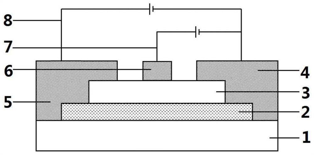
[0040] refer to figure 1 As shown in the figure, a schematic structural diagram of a TNW field effect memristor provided by an embodiment of the present invention, the memristor includes a substrate 1 on which a memristive layer 2 is arranged, and the memristive layer 2 is a two-dimensional Tellurene nanowire; the middle part of the two-dimensional tellurene nanowire is covered by an insulating layer 3, and its two ends are kept exposed; the exposed two ends of the two-dimensional tellurene nanowire and the surface of the insulating layer 3 Metal electrodes are respectively provided; the metal electrode 4 is the drain electrode, the metal electrode 5 is the source electrode, and the metal electrode 6 is the gate electrode. The metal electrodes 5 and 6 are electrically connected to the metal electrodes 4 through wires 7 and 8, respectively.

[0041] The field effect memristor based on two-dimensional tellurene nanowires and the fabrication method thereof in this embodiment are...


PUM

PropertyMeasurementUnit
lengthaaaaaaaaaa
widthaaaaaaaaaa
heightaaaaaaaaaa

Abstract

The invention relates to a field effect memristor based on two-dimensional tellurene nanowires and a manufacturing method thereof, belonging to the technical field of microelectronics. The memristor of the present invention includes a substrate on which a memristive layer is provided, and the memristive layer is a two-dimensional tellurene nanowire; the middle of the two-dimensional tellurene nanowire is covered by an insulating layer , the two ends of the two-dimensional tellurene nanowire are kept exposed; the exposed two ends of the two-dimensional tellurene nanowire and the surface of the insulating layer are respectively provided with metal electrodes. The resistance of the field effect memristor of the present invention is regulated by the field voltage, and the resistance changes by 3 orders of magnitude. The brief effect of the field voltage has a non-volatile effect on the resistance of the device, resulting in a resistance change of 1 order of magnitude. The memristor can not only use its field effect to realize logic operations, but also use its resistance memory function. The memristor of the present invention is simple in structure, simple in preparation, fast in response speed and superior in performance, is an integrated device of storage and calculation, and has broad application prospects.

Description

technical field [0001] The invention relates to the technical field of microelectronics, in particular to a field effect memristor based on two-dimensional tellurene nanowires and a manufacturing method thereof. Background technique [0002] Since the successful preparation of two-dimensional tellurene in 2017, because of its many excellent properties, it has great potential in the application of electronic devices such as photodetectors. However, most studies focus on tellurium nanosheets, and there are few related studies on 2D tellurene nanowires TNW, while 2D tellurene nanowires TNW have the same structure and similar properties as tellurium nanosheets, but their smaller size And the unique boundary characteristics make it have wider application prospects. In the traditional computer architecture, data storage and data processing are separated, which takes a long time and consumes a lot of power. The integrated storage and computing chip is expected to greatly improve t...

Claims


Application Information

Patent Timeline
Patent Type & Authority Patents(China)
IPC IPC(8): H01L45/00
CPCH10N70/841H10N70/011H10N70/8828
Inventor 姜昱丞龚帅楠高炬
Owner SUZHOU UNIV OF SCI & TECH
Why Eureka
Try Eureka