DMD circuit board and DLP light machine module

A technology of optical-mechanical modules and circuit boards, which is applied in the field of digital optical processing, can solve problems such as multiple process steps, DMD circuit board stacking, board thickness, board material and other parameter limitations, and product reliability risks.

Active Publication Date: 2022-01-21
GOERTEK OPTICAL TECH CO LTD
View PDF7 Cites 0 Cited by
  • Summary
  • Abstract
  • Description
  • Claims
  • Application Information

AI Technical Summary

Problems solved by technology

[0004] At present, in order to meet the needs of light, thin and miniaturized products, DMD circuit boards are mostly designed with FPC (Flexible Printed Circuit, flexible circuit board). However, due to the limitation of process capability, the number of layers of FPC cannot be equal to the number of layers of conventional PCB. The parameters such as the stack structure, board thickness, and board material of the DMD circuit board are subject to many restrictions, which will adversely affect the anti-ESD (Electro-Static discharge, electrostatic discharge) performance and EMI (Electromagnetic Interference, electromagnetic interference) performance of the DMD circuit board. impact, ultimately leading to poor signal integrity on the DMD board
[0005] In the prior art, the anti-ESD and anti-EMI performance of the product is usually improved by wrapping conductive cloth on the outside of the DMD circuit board or additionally mounting conductive materials such as conductive foam on the surface. However, this method is not only a process step Many, and the production cost is high, and at the same time, it has an adverse effect on the signal integrity of the DMD circuit board, and there is a risk in product reliability

Method used


Image

  • DMD circuit board and DLP light machine module
  • DMD circuit board and DLP light machine module
  • DMD circuit board and DLP light machine module

Examples


Embodiment Construction

[0027] The following will clearly and completely describe the technical solutions in the embodiments of the present invention with reference to the accompanying drawings in the embodiments of the present invention. Obviously, the described embodiments are only some, not all, embodiments of the present invention. Based on the embodiments of the present invention, all other embodiments obtained by persons of ordinary skill in the art without making creative efforts belong to the protection scope of the present invention.

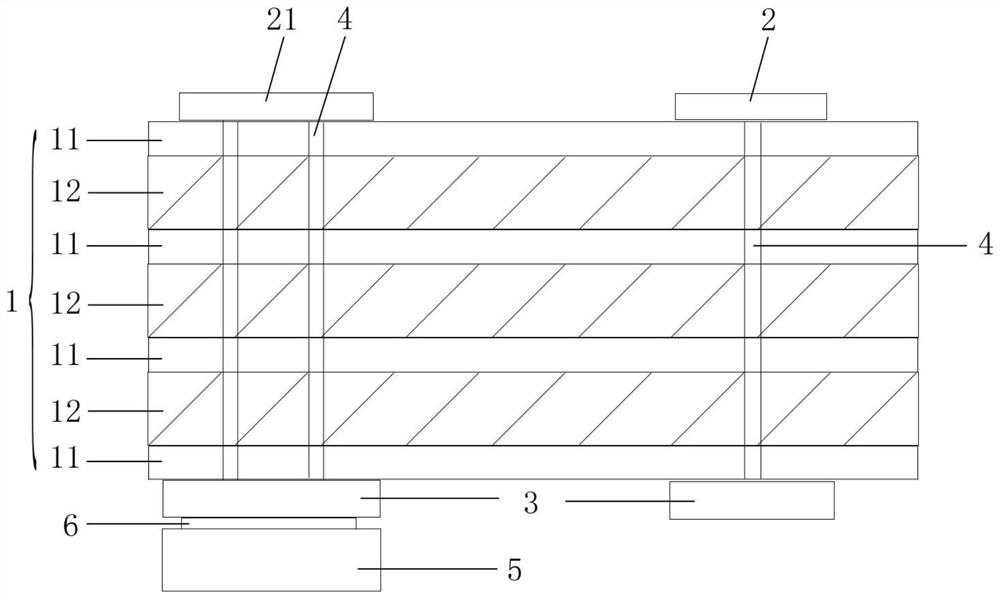
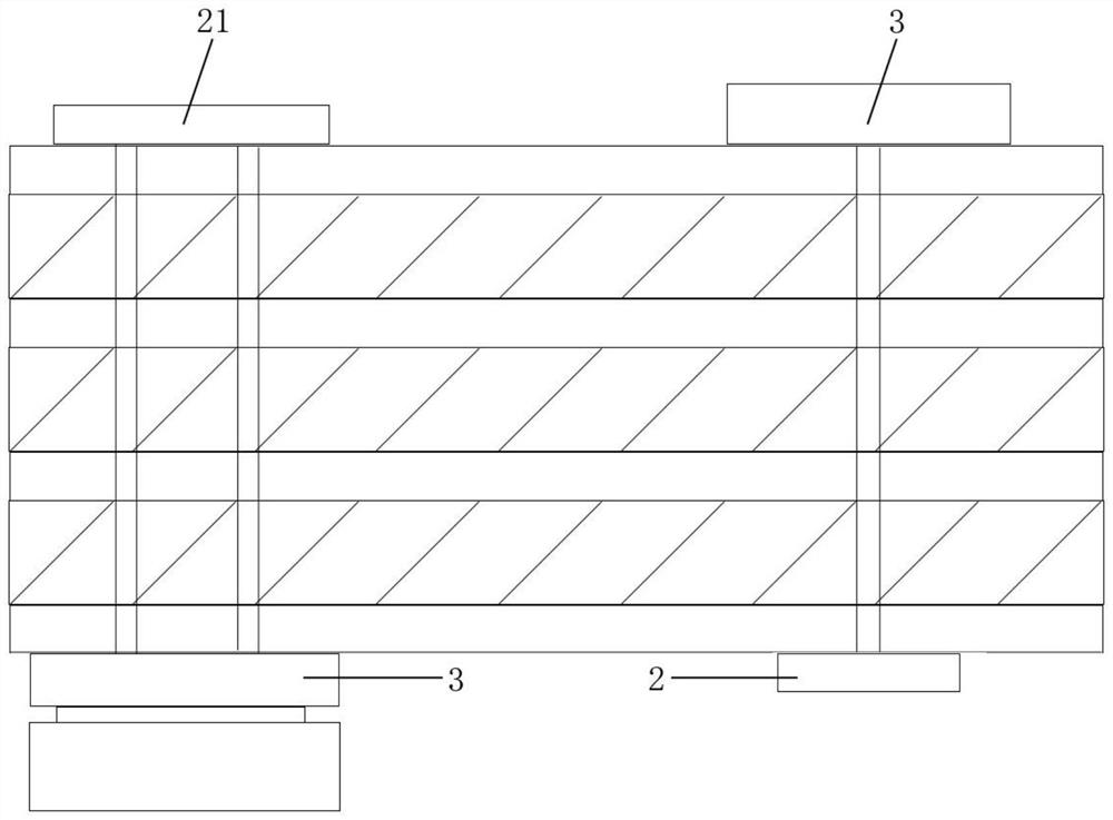
[0028] Please refer to figure 1 , figure 1 It is a schematic diagram of the overall structure of a specific embodiment provided by the present invention.

[0029] In a specific embodiment provided by the present invention, the DMD circuit board mainly includes a substrate body 1 , electronic components 2 , a reinforcing plate 3 and via holes 4 .

[0030] Among them, the substrate body 1 is the main structure of the DMD circuit board, mainly used for installi...


PUM


Abstract

The invention discloses a DMD circuit board, which comprises a substrate body, a plurality of electronic components arranged on one side surface of the substrate body, and a plurality of reinforcing plates arranged on the other side surface of the substrate body and corresponding to the positions of the electronic components; and each electronic component is connected with the corresponding reinforcing plate through a ground via hole, and each reinforcing plate is electrically connected with a grounding shell of the DLP light machine module. Thus, the electronic component is connected with the reinforcing plate through the via hole with the ground property, and then is connected with the grounding shell of the DLP optical machine module through the reinforcing plate, so that the DMD circuit board is directly grounded through the reinforcing plate and the grounding shell (the whole machine), compared with the prior art, the electrostatic discharge path is short, the electrostatic discharge path is direct, the ESD resistance and EMI resistance of the DMD circuit board can be enhanced, and then the signal integrity of the DMD circuit board is improved with high efficiency and low cost. The invention further discloses a DLP light machine module, and the beneficial effects of the DLP light machine module are as mentioned above.

Description

technical field [0001] The invention relates to the technical field of digital light processing, in particular to a DMD circuit board. The invention also relates to a DLP optical machine module. Background technique [0002] DLP (Digital Light Processing, digital light processing) technology is an imaging technology, mainly through digital processing of image signals, and then through DMD (Digital Micromirror Device, digital micromirror chip) to realize the projection display of visual digital information. [0003] DMD is a key component of DLP optical-mechanical module, and the quality of DMD design directly affects the electrical and optical performance of DLP optical-mechanical module. DMD is a matrix composed of a large number of microlenses arranged on the chip, each microlens controls a pixel in the projected picture, and the number of microlenses matches the resolution of the projected picture. These micromirrors can change the angle quickly under the control of dig...

Claims


Application Information

Patent Timeline
Patent Type & Authority Applications(China)
IPC IPC(8): G03B21/00G03B21/14G03B21/16
CPCG03B21/008G03B21/16G03B21/145
Inventor 高文刚马菲菲
Owner GOERTEK OPTICAL TECH CO LTD
Why Eureka
Try Eureka