A Gaas-based light-emitting diode and its manufacturing method

A technology for light-emitting diodes and a manufacturing method, which is applied to electrical components, circuits, semiconductor devices, etc., can solve problems such as poor ESD performance and affect crystal quality, and achieve the effect of improving anti-ESD performance and solving poor ESD performance.

Active Publication Date: 2018-08-31
QUANZHOU SANAN SEMICON TECH CO LTD
View PDF7 Cites 0 Cited by
  • Summary
  • Abstract
  • Description
  • Claims
  • Application Information

AI Technical Summary

Problems solved by technology

This method has been widely used, however, the ESD performance of this structure becomes poor under the small size chip
The study found that the main reason is that using this transition method still produces more dislocation lines at the interface, and the dislocation lines extend to the GaP current spreading layer, which affects the crystal quality

Method used


Image

  • A Gaas-based light-emitting diode and its manufacturing method
  • A Gaas-based light-emitting diode and its manufacturing method
  • A Gaas-based light-emitting diode and its manufacturing method

Examples


Embodiment 1

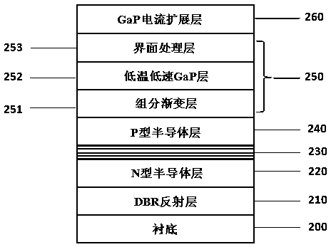
[0048] Such as figure 2 As shown, this embodiment provides a method for manufacturing a GaAs-based light-emitting diode, including the following process steps: using metal organic chemical vapor deposition (MOCVD) to epitaxially grow a DBR reflective layer 210, an N-type semiconductor layer 220, Quantum well light-emitting layer 230, P-type semiconductor layer 240, transition layer 250 and GaP current spreading layer 260, wherein transition layer 250 includes composition gradient layer 251, low temperature and low speed GaP layer 252, interface treatment layer 253, GaP current spreading layer 260 uses same growth temperature.

[0049] The manufacturing method of the GaAs-based light-emitting diode described in the present invention uses high-purity hydrogen (H2) as the carrier gas, trimethylgallium (TMGa), trimethylaluminum (TMAl), trimethylindium (TMIn), arsine (AsH3) and phosphine (PH3) are used as Ga, Al, In, As, and P sources respectively, and silane (Si2H6) and dimagnes...

Embodiment 2

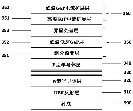
[0062] This embodiment is different from Embodiment 1 in that: the GaP current spreading layer is prepared by high temperature first and then low temperature. After the interface treatment layer is grown, the temperature is raised abruptly to grow a layer of high-temperature GaP, and then the temperature is suddenly lowered to the required growth temperature of the GaP current spreading layer for growth.

[0063] Such as image 3 with 4 As shown, a DBR reflective layer 310, an N-type semiconductor layer 320, a quantum well light-emitting layer 330, a P-type semiconductor layer 340, a transition layer 350, and a GaP current spreading layer are epitaxially grown sequentially on a substrate 300 by metal organic chemical vapor deposition (MOCVD). Layer 360. The transition layer 350 includes a graded composition layer 351 , a low temperature and low velocity GaP layer 352 , and an interface treatment layer 353 . The GaP current spreading layer includes a high temperature GaP cur...


PUM


Abstract

A GaAs-based light emitting diode and manufacturing method therefor, the diode sequentially comprising a substrate (200), a DBR reflective layer (210), an N-type semiconductor layer (220), a quantum well light emitting layer (230), a P-type semiconductor layer (240), a transition layer (250) and a GaP current spreading layer (260); the transition layer (250) comprises a graded component layer (251), a low-temperature low-speed GaP layer (252) and an interface processing layer (253), and the GaP current spreading layer (260) is of a mode wherein high-temperature growth is followed by low-temperature growth. By means of the transition layer (250), a dislocation line can be effectively pressed at an interface. A high-temperature GaP current spreading layer is connected with the interface processing layer (253) to further press a dislocation line which extends into an interface layer in the high-temperature GaP current spreading layer, so as to provide a good foundation for the growth of a subsequent high-quality GaP current spreading layer.

Description

technical field [0001] The invention relates to the field of semiconductor optoelectronic devices, in particular to a GaAs-based light-emitting diode and a manufacturing method thereof. Background technique [0002] In recent years, LED has developed rapidly and has been widely used in the market. In the field of LED technology, brightness enhancement has always been a research hotspot, and breakthroughs have been made. In GaAs-based LEDs, the light extraction efficiency is mainly improved by flip-chip structure, DBR reflective structure or increasing current injection density. For example, in Chinese Patent No. 201010260023.8, a vertical light-emitting diode with a current blocking structure is proposed for brightness improvement, and a hollow current blocking structure with air as the medium is formed between the electrode and the patterned GaP window layer to reduce the current flow from The bottom of the electrode expands, and more current spreads from around the GaP w...

Claims


Application Information

Patent Timeline
Patent Type & Authority Patents(China)
IPC IPC(8): H01L33/00H01L33/12H01L33/14
CPCH01L33/00H01L33/12H01L33/14
Inventor 郑元宇郑建森伍明跃周启伦邱财华罗宵林峰李水清吴超瑜蔡坤煌
Owner QUANZHOU SANAN SEMICON TECH CO LTD
Why Eureka
Try Eureka