Method for regulating and controlling doping characteristic of two-dimensional material through thickness of atomic layer

A technology of two-dimensional materials and doping characteristics, which is applied in the field of regulation and control of doping characteristics of two-dimensional atomic layer materials. Realize the effect of doping type and doping stability

Pending Publication Date: 2022-01-21
SHANGHAI INST OF TECHNICAL PHYSICS - CHINESE ACAD OF SCI
View PDF3 Cites 0 Cited by
  • Summary
  • Abstract
  • Description
  • Claims
  • Application Information

AI Technical Summary

Problems solved by technology

However, this doping method often makes the two-dimensional atomic layer material too heavily doped, and it is difficult to achieve controllable doping.
Moreover, as the electric field of the device is added, the metal atoms between the layers will move, making it difficult to maintain the doping characteristics of the two-dimensional atomic layer material for a long time.
Gate voltage regulated doping is the doping type of two-dimensional atomic layer materials controlled by external local gate voltage. Although it can be maintained for a long time, it needs to be maintained with an external voltage and consumes a lot of power.
Therefore, the controllable doping of 2D atomic layer materials remains a great challenge and problem to be solved

Method used


Image

  • Method for regulating and controlling doping characteristic of two-dimensional material through thickness of atomic layer
  • Method for regulating and controlling doping characteristic of two-dimensional material through thickness of atomic layer
  • Method for regulating and controlling doping characteristic of two-dimensional material through thickness of atomic layer

Examples


Embodiment Construction

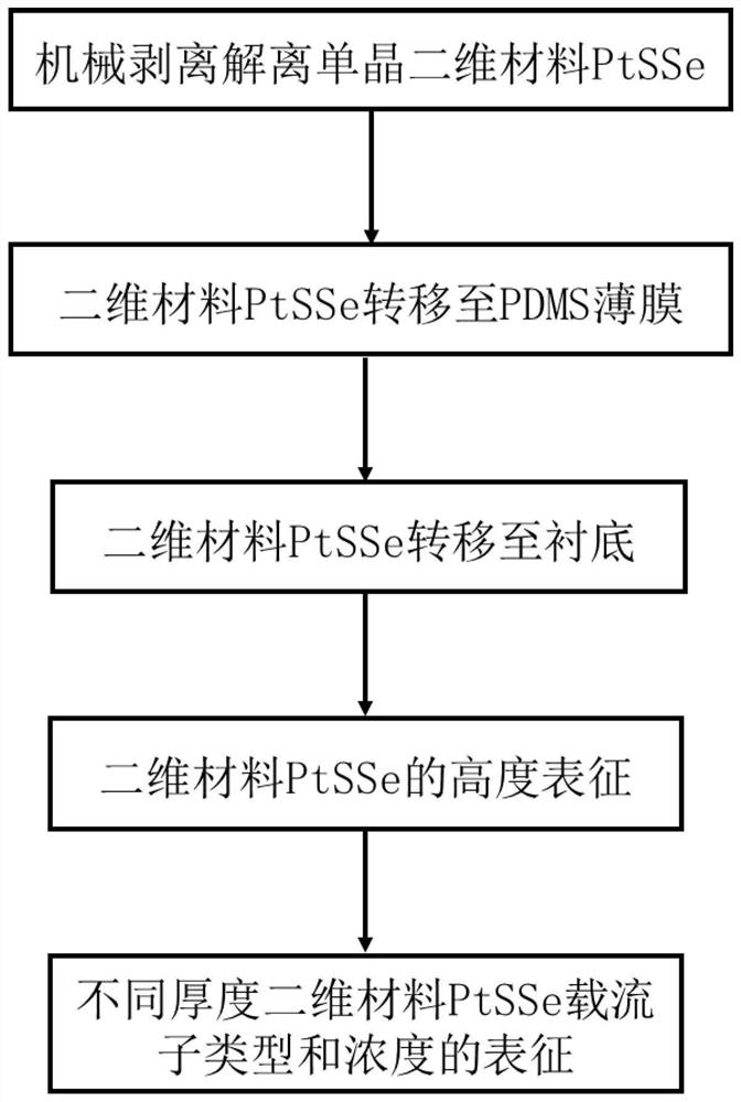
[0018] The specific embodiments of the present invention will be described in detail below in conjunction with the accompanying drawings, but the present invention is not limited to the following embodiments. The drawings use imprecise ratios and simplified forms, which are only used to facilitate and clearly illustrate the specific flow and operation process of the embodiment of the present invention.

[0019] 1. Please refer to figure 1 , figure 1 The method for controlling the doping characteristics of two-dimensional materials by atomic layer thickness is shown, and the specific method flow is as follows:

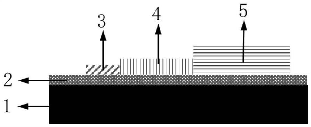
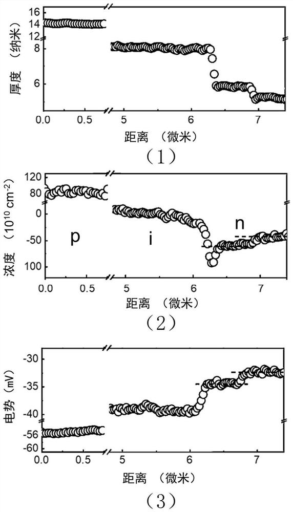
[0020] Step 1: Mechanical exfoliation to dissociate the single-crystal two-dimensional material PtSSe. The size of chemical vapor transport growth is 1×1mm 2 The single crystal two-dimensional atomic layer semiconductor material PtSSe is taken out and put on the thermal release tape. After folding and tearing the tape in half 6 times, the two-dimensional atomic laye...


PUM

PropertyMeasurementUnit
thicknessaaaaaaaaaa
thicknessaaaaaaaaaa
thicknessaaaaaaaaaa

Abstract

The invention discloses a method for regulating and controlling the PtSSe doping characteristic of a two-dimensional material through the thickness of an atomic layer. According to the method, the two-dimensional material PtSSe is thinned through mechanical stripping, the doping type of the two-dimensional atomic layer material is converted into an i type from a p type and then into an n type along with the reduction of the thickness of the atomic layer, and the carrier concentration is changed from 1012 cm<-2 > to 1011 cm<-2 >. The key point of controllable doping is to prepare two-dimensional materials with different thicknesses, and along with the change of the thickness of the two-dimensional material, the stress in the material changes, so that the PtSSe point defect type of the two-dimensional material changes, and the doping of the two-dimensional material is realized. Moreover, the thickness of the two-dimensional material PtSSe is only changed by 0.8 nm, and the doping concentration is obviously changed, so that the doping of the atomic layer thickness of the two-dimensional material is realized. The method has the advantages that the continuous change of the doping type and the doping concentration of the two-dimensional atomic layer semiconductor material is simply and controllably realized by the monatomic layer without damage.

Description

technical field [0001] The invention relates to a method for controlling the doping type and doping concentration of a two-dimensional material by atomic layer thickness, in particular to a controllable, simple and non-destructive method for controlling the doping characteristics of a two-dimensional atomic layer material. Background technique [0002] Two-dimensional materials are a class of materials that are atomically thick. For semiconductors that are two-dimensional atomic layer materials, each layer consists of three rows of atoms. Its unique crystal arrangement and crystal structure make it have peculiar electrical, optical and magnetic properties, and then it is widely studied, providing a feasible way to change the basic structure of current devices and solve the problems of electronic and optoelectronic devices . Doping is the most fundamental and important step in the semiconductor process, determining the structure and performance of later device designs. The ...

Claims


Application Information

Patent Timeline
Patent Type & Authority Applications(China)
IPC IPC(8): H01L31/18H01L31/032H01L31/075
CPCH01L31/1896H01L31/0321H01L31/075Y02E10/548Y02P70/50
Inventor 王振胡伟达王鹏谢润章张莉丽王芳仲方贺婷陈效双陆卫
Owner SHANGHAI INST OF TECHNICAL PHYSICS - CHINESE ACAD OF SCI
Why Eureka
Try Eureka