LinkPort communication system and method based on FPGA

A communication method and communication system technology, applied in the field of FPGA-based LinkPort communication system, can solve problems such as not detailed description, high FPGA performance, inability to apply low-end FPGA, etc., to increase timing margin, optimize timing, and facilitate timing Convergence effect

Active Publication Date: 2022-01-21
750 TEST SITE OF CHINA SHIPBUILDING IND CORP
View PDF3 Cites 0 Cited by
  • Summary
  • Abstract
  • Description
  • Claims
  • Application Information

AI Technical Summary

Problems solved by technology

However, the performance of the FPGA used in this article is high, and it is stated that manual optimization is required in the layout and routing stage. At the same time, the physical layer of the TS201 LinkPort interface itself uses high-speed LVDS signals, and finally achieves a bus frequency of 300MHz. However, the solution is the key to how to achieve high performance. Design is not exhaustive and cannot be applied to low-end FPGAs

Method used


Image

  • LinkPort communication system and method based on FPGA
  • LinkPort communication system and method based on FPGA
  • LinkPort communication system and method based on FPGA

Examples


Embodiment Construction

[0043] The present invention will be described in further detail below in conjunction with the accompanying drawings.

[0044] ODDR / IDDR: FPGA primitives.

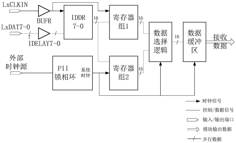
[0045] The present invention provides an FPGA-based LinkPort communication system, comprising: a sending module, a receiving module, a phase-locked loop circuit PLL connected to an external clock source, and the phase-locked loop circuit PLL is used to receive an external clock source and generate a bus input clock The 0° and 270° clocks have the same frequency, the 0° clock is used as the system clock, and the 270° clock is used to drive data output.

[0046] Such as image 3 As shown, the receiving module includes: a local clock buffer BUFR connected to the bus input clock LxCLKIN, a delay unit IDELAY connected to the bus data LxDAT, an IDDR circuit connected to the bus input clock LxCLKIN and the bus data LxDAT, and a phase-locked loop circuit The register group connected to the PLL and the IDDR circuit, and the data ...


PUM


Abstract

The invention discloses a LinkPort communication system and method based on an FPGA, and the method comprises the steps: a receiving step: receiving a bus input clock by a receiving module, taking the bus input clock as a trigger clock of an IDDR circuit, capturing bus data, converting the bus data into single-rate data, capturing data outputted by the IDDR circuit by using a register set, storing data captured by a register group into a data buffer area, and when data needs to be sent, outputting the data from the data buffer area by a receiving module in a data frame form, and entering a sending step: generating 0-degree and 270-degree clocks with the same frequency as a bus clock by a phase-locked loop circuit; enabling the 0-degree clock driving data ODDR circuit to receive the data and generate the bus output data, and enabling the 270-degree clock driving clock ODDR circuit to generate a bus output clock; after sending of one frame of data is completed, carrying out the sending of the next frame of data. Therefore, the maximum 125MHz bus communication rate supported by the LinkPort protocol is realized, the time sequence margin is increased, and the method can be applied to a relatively low-end FPGA.

Description

technical field [0001] The invention relates to the field of FPGA technology, in particular to an FPGA-based LinkPort communication system and method. Background technique [0002] Such as figure 1 As shown, the LinkPort interface is in half-duplex mode, and it can also be used as a simplex mode. The essence of the link layer of the protocol is the source synchronous interface (Source Synchronous Interface) of DDR (Double Data Rate, double rate) transmission. With 128bit data frame as the transmission granularity, each frame of data requires 8 bus clocks. Each LinkPort interface has both an input clock and an output clock signal. The clock signal is not only used to synchronize data, but also used to complete the communication control function. figure 2 Shown is the LinkPort link layer communication protocol (only a partial illustration). In the figure, the LxCLKOUT output clock is a discontinuous clock, which is used for bus request (TOKEN REQUEST) and for synchronizing...

Claims


Application Information

Patent Timeline
Patent Type & Authority Applications(China)
IPC IPC(8): H04J3/06H04L12/40G06F9/54G06F1/12
CPCH04J3/0682H04L12/40G06F9/544G06F1/12Y02D10/00
Inventor 纳杰斯李运周岳雷陈泽锐
Owner 750 TEST SITE OF CHINA SHIPBUILDING IND CORP
Why Eureka
Try Eureka