Display substrate, preparation method thereof and display device
A technology for displaying substrates and polar plates, which is applied in the direction of electrical components, electrical solid devices, circuits, etc., can solve the problems of complex process flow, high production cost, and many times of patterning processes, so as to reduce the number of processes, reduce process costs, The effect of shortening the process time
- Summary
- Abstract
- Description
- Claims
- Application Information
AI Technical Summary
Problems solved by technology
Method used
Image

Examples
Embodiment Construction
[0082] The embodiments herein may be embodied in many different forms. Those skilled in the art can easily understand the fact that the implementation and contents can be changed into various forms without departing from the gist and scope of the present disclosure. Therefore, the present disclosure should not be interpreted as being limited only to the contents described in the following embodiments. In the case of no conflict, the embodiments in the present disclosure and the features in the embodiments can be combined arbitrarily with each other.
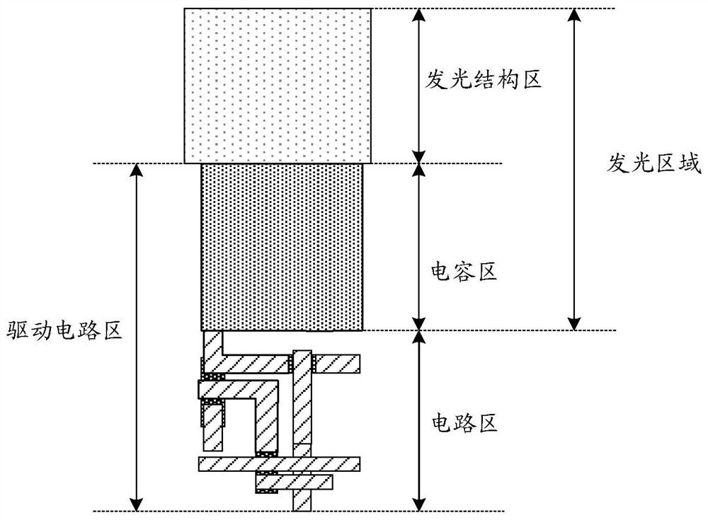
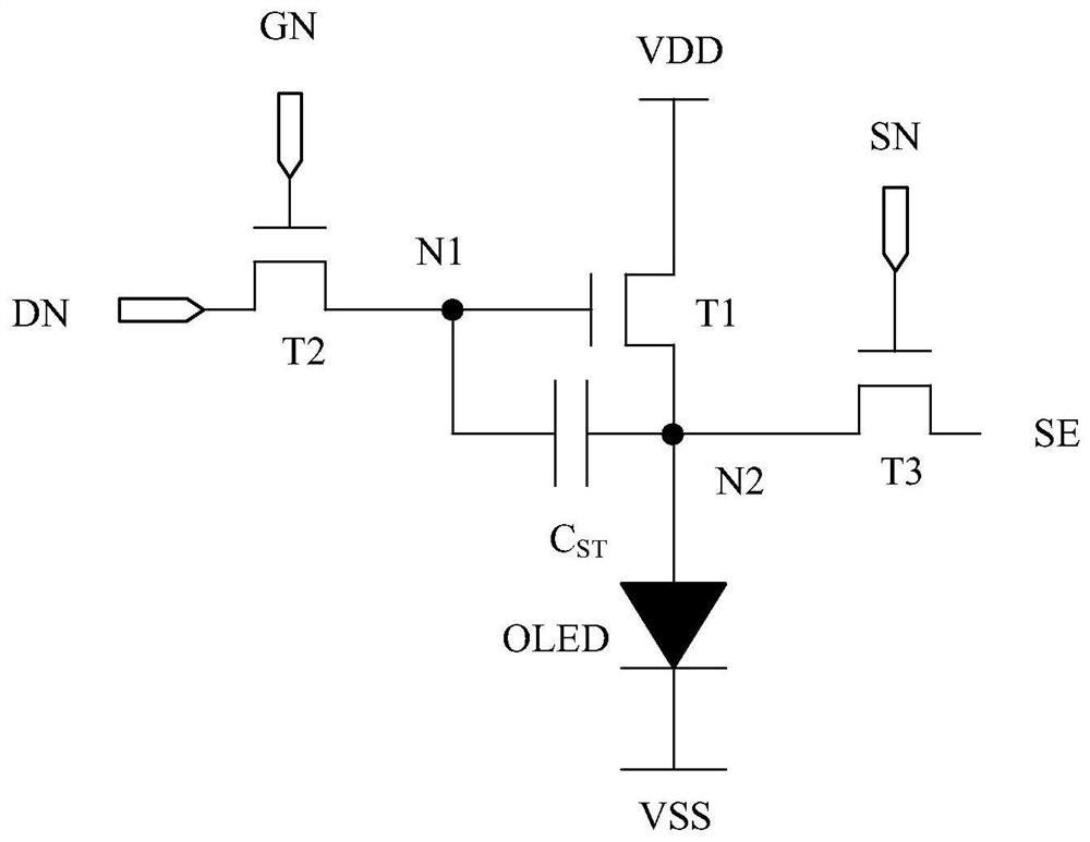
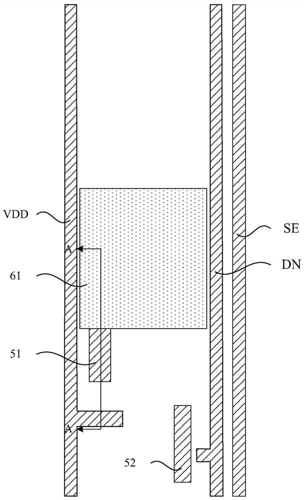
[0083] In the drawings, the size of constituent elements, the thickness of layers, or regions may be exaggerated for the sake of clarity. Therefore, any implementation of the present disclosure is not necessarily limited to the dimensions shown in the drawings, and the shapes and sizes of components in the drawings do not reflect true scales. In addition, the drawings schematically show ideal examples, and any implementation of...
PUM
 Abstract
Description
Claims
Application Information
 - R&D
- Intellectual Property
- Life Sciences
- Materials
- Tech Scout
- Unparalleled Data Quality
- Higher Quality Content
- 60% Fewer Hallucinations
Browse by: Latest US Patents, China's latest patents, Technical Efficacy Thesaurus, Application Domain, Technology Topic, Popular Technical Reports.
© 2025 PatSnap. All rights reserved.Legal|Privacy policy|Modern Slavery Act Transparency Statement|Sitemap|About US| Contact US: help@patsnap.com