

High-stability light emitting diode chip and manufacturing method thereof
A light-emitting diode, high-stability technology, used in electrical components, circuits, semiconductor devices, etc., can solve problems such as interface corrosion, chip reliability decline, electrode blocking of light, etc., to achieve a large contact area, improve reliability, and tightness. Good results
- Summary
- Abstract
- Description
- Claims
- Application Information
AI Technical Summary
Problems solved by technology
Method used
Image

Examples
Embodiment Construction
[0042] In order to make the purpose, technical solution and advantages of the present disclosure clearer, the implementation manners of the present disclosure will be further described in detail below in conjunction with the accompanying drawings.
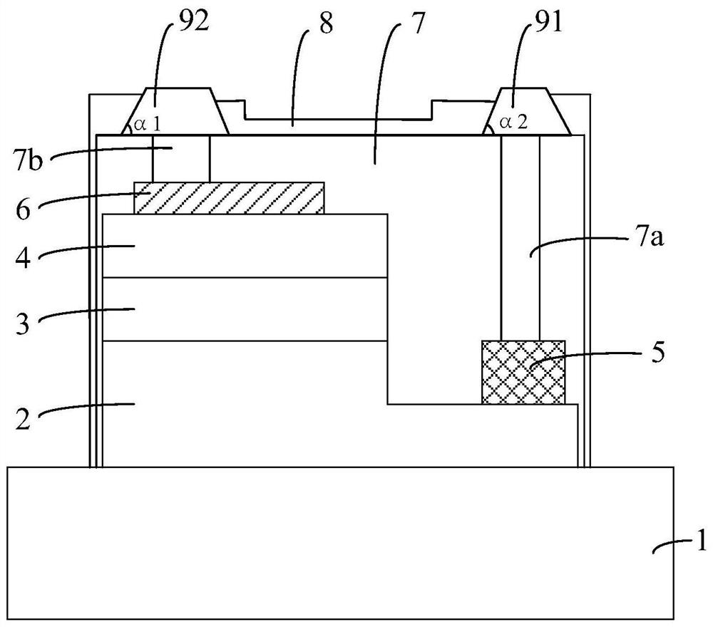
[0043] figure 1 It is a schematic structural diagram of a highly stable light-emitting diode chip provided by an embodiment of the present disclosure, as shown in figure 1 As shown, the highly stable LED chip 100 includes a substrate 1 , an N-type semiconductor layer 2 , an active layer 3 , a P-type semiconductor layer 4 , an N-type electrode 5 , a P-type electrode 6 , an insulating layer 7 and solder joints. N-type semiconductor layer 2 , active layer 3 , and P-type semiconductor layer 4 are sequentially stacked on surface 1 a of substrate 1 . The P-type semiconductor layer 4 is provided with a groove extending to the N-type semiconductor layer 2 . The N-type electrode 5 is arranged on the N-type semiconductor layer 2 in the gro...
PUM
| Property | Measurement | Unit |
|---|---|---|
| Total thickness | aaaaa | aaaaa |
Abstract
Description
Claims
Application Information