CMOS image sensor and manufacturing method

An image sensor and manufacturing method technology, applied in the direction of electric solid-state devices, semiconductor devices, radiation control devices, etc., can solve the problems of far away from the doping concentration peak, increase the TG tube, and unfavorable imaging quality, so as to expand the width of the depletion region , Eliminate reset noise and improve image quality

Pending Publication Date: 2022-02-01
SHANGHAI HUALI MICROELECTRONICS CORP
View PDF0 Cites 1 Cited by
  • Summary
  • Abstract
  • Description
  • Claims
  • Application Information

AI Technical Summary

Problems solved by technology

The following two methods are usually used to increase the width of the depletion region of the PPD: one is to increase the voltage of the TG tube (Transfer Gate, transfer switch), but it will also cause band-to-band tunneling (Band-to -BandTunneling, BBT) leakage, that is, the dark current is increased synchronously, which is not conducive to the improvement of imaging quality, and increasing the voltage of the TG tube will also increase the design difficulty of the peripheral circuit; the second is to increase the N-type buried layer in the PPD Although it can be formed in one step by increasing the energy of ion implantation when forming the N-type buried layer, high-energy implantation will cause the peak doping concentration of the N-type buried layer in the PPD to be far away from the TG tube, which is not conducive to the charge ( Photogenerated electrons) transfer, and the deeper N-type buried layer will also cause the free electrons in the depletion region before exposure to be difficult to be depleted, both of which limit the charge transfer efficiency (Charge Transfer Efficiency, CTE ), causing serious image smearing problems

Method used


Image

  • CMOS image sensor and manufacturing method
  • CMOS image sensor and manufacturing method
  • CMOS image sensor and manufacturing method

Examples


Embodiment Construction

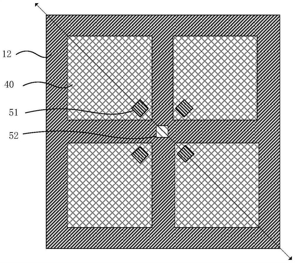
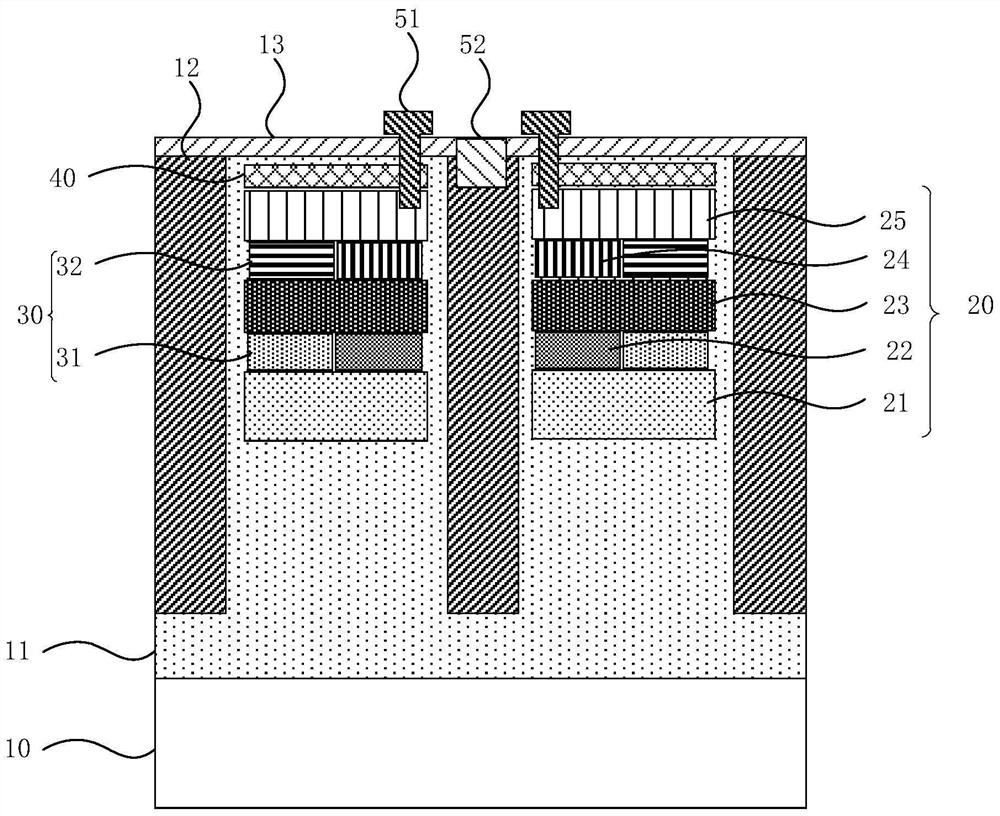
[0029] In order to make the purpose, advantages and features of the present invention clearer, the present invention will be further described in detail below in conjunction with the accompanying drawings and specific embodiments. It should be noted that the drawings are all in very simplified form and not drawn to scale, and are only used to facilitate and clearly assist the purpose of illustrating the embodiments of the present invention. In addition, the structures shown in the drawings are often a part of the actual structure. In particular, each drawing needs to display different emphases, and sometimes uses different scales.

[0030] As used in the present invention, the singular forms "a", "an" and "the" include plural objects, the term "or" is usually used in the sense of including "and / or", and the term "several" Usually, the term "at least one" is used in the meaning of "at least one", and the term "at least two" is usually used in the meaning of "two or more". In a...


PUM


Abstract

The invention provides a CMOS image sensor and a manufacturing method. The CMOS image sensor comprises a P-type substrate, a P-type epitaxial layer and a plurality of pixel units, wherein the P-type epitaxial layer is formed on the P-type substrate, an N-type buried layer, a P-type clamping layer, the P-type buried layer and the P-type epitaxial layer form a clamping photodiode, the N-type buried layer, the P-type clamping layer and the P-type buried layer are all formed in the P-type epitaxial layer, the P-type clamping layer is formed above the N-type buried layer, the P-type buried layer is embedded into the N-type buried layer, the P-type buried layer comprises at least two P-type sub-buried layers, and the at least two P-type sub-buried layers are distributed in the depth direction of the P-type epitaxial layer. By using the P-type buried layer formed in the N-type buried layer, the width of a depletion region of the clamping photodiode is expanded, the PN junction capacitance is increased, and the quantum efficiency and the full well capacity of the pixel unit are improved, so that the sensitivity and the imaging performance of a pixel unit are improved, the N-type buried layer is easier to deplete before exposure, and the reset noise is reduced.

Description

technical field [0001] The invention relates to the field of integrated circuits, in particular to a CMOS image sensor and a manufacturing method. Background technique [0002] With the development of CMOS image sensors, the resolution per unit area has repeatedly reached new highs, which will inevitably lead to the continuous reduction of the size and pitch of pixel units. As the photosensitive unit of the pixel unit, the clamped photodiode (Pinned Photodiode, PPD) is limited by the size of the pixel unit, which affects its collection of photogenerated electrons and reduces the number of electrons collected per unit time, resulting in The sensitivity (such as quantum efficiency QE, Quantum Efficiency) of the CMOS image sensor decreases. [0003] For this reason, on the premise that the resolution of the pixel unit of the CMOS image sensor has repeatedly reached new heights, it is the key to maintain or improve the quantum efficiency of the pixel unit by designing a high-qu...

Claims


Application Information

Patent Timeline
Patent Type & Authority Applications(China)
IPC IPC(8): H01L27/146
CPCH01L27/14643H01L27/14603H01L27/14683
Inventor 王鹏
Owner SHANGHAI HUALI MICROELECTRONICS CORP
Why Eureka
Try Eureka