
Method for improving hot melting thickness uniformity of PCB

A PCB board with uniform thickness technology, applied in laminated printed circuit boards, multi-layer circuit manufacturing, circuit lamination, etc., can solve the problems of poor fluidity, unstable temperature, and uneven thickness of the board edge glue, and achieve improved The uniformity of hot melt thickness, the reduction of the probability of scrapping, and the effect of uniform thickness

Pending Publication Date: 2022-02-22
APCB ELECTRONICS SHENZHEN CO LTD
View PDF0 Cites 0 Cited by
  • Summary
  • Abstract
  • Description
  • Claims
  • Application Information

AI Technical Summary

Problems solved by technology

[0002] In the lamination production process of the PCB (Printed Circuit Board) board to be fused, it is necessary to overlap the prepreg and the substrate to form the PCB board to be fused, and set a hot melt block on the edge of the board, and the hot melt machine Through the contact between the hot-melt chuck and the heating sheet and the surface of the hot-melt block, the heated hot-melt block makes the prepreg gel and fuse with the substrate. During the heating process, due to the influence of the heat accumulation of the plate, the prepreg and the substrate are repeated Fast heat transfer will increase its glue flow or cause temperature instability, resulting in uneven heating in the area of ​​the hot melt block, resulting in uneven thickness. This area will form a height difference, and the fluidity of the edge glue during pressing is not good. , forming wrinkles, increasing the probability of PCB board scrapping

Method used


Image

  • Method for improving hot melting thickness uniformity of PCB
  • Method for improving hot melting thickness uniformity of PCB

Examples


Embodiment Construction

[0024] The following will clearly and completely describe the technical solutions in the embodiments of the present invention with reference to the accompanying drawings in the embodiments of the present invention. Obviously, the described embodiments are only some of the embodiments of the present invention, not all of them. Based on the embodiments of the present invention, all other embodiments obtained by persons of ordinary skill in the art without creative efforts fall within the protection scope of the present invention.

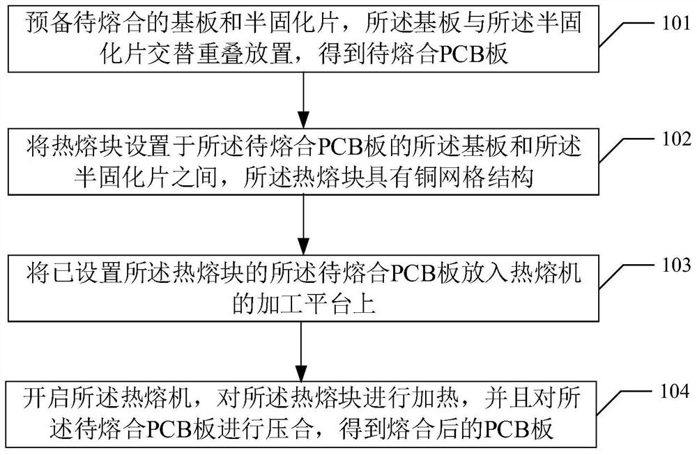
[0025] Such as figure 1 As shown, it is a schematic flow diagram of a method for improving the uniformity of PCB heat-melt thickness in one embodiment, the method comprising:

[0026] Step 101, prepare the substrate to be fused and the prepreg, and place the substrate and the prepreg alternately to obtain a PCB to be fused;

[0027] In the embodiment of the present application, a substrate and a prepreg are stacked to form a ply structure, and the pl...


PUM


Abstract

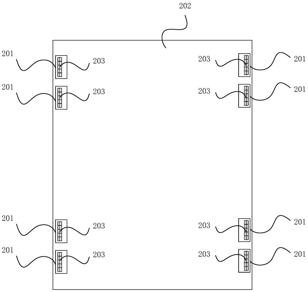
The embodiment of the invention discloses a method for improving the hot melting thickness uniformity of a PCB. The method comprises the steps of: preparing substrates and prepregs to be fused, enabling the substrates and the prepregs to be alternately overlapped to obtain a to-be-fused PCB, enabling hot melting blocks of a copper grid structure to be disposed between the substrates and the prepregs of the to-be-fused PCB, putting the to-be-fused PCB with the hot melting blocks on a processing platform of a hot melting machine, starting the hot melting machine to heat the hot melting blocks, and pressing the to-be-fused PCB to obtain a fused PCB. The hot melting blocks of a copper grid structure are arranged between the substrates and the prepregs of the to-be-fused PCB, and the to-be-fused PCB is heated and pressed, so that the hot melting block area is heated uniformly, the produced PCB is uniform in thickness and not easy to wrinkle, and the probability of scrapping of the PCB is reduced.

Description

technical field [0001] The invention relates to the technical field of PCB printed circuit board production, in particular to a method for improving the uniformity of thermal melting thickness of a PCB board. Background technique [0002] In the lamination production process of the PCB (Printed Circuit Board) board to be fused, it is necessary to overlap the prepreg and the substrate to form the PCB board to be fused, and set a hot melt block on the edge of the board, and the hot melt machine Through the contact between the hot-melt chuck and the heating sheet and the surface of the hot-melt block, the heated hot-melt block makes the prepreg gel and fuse with the substrate. During the heating process, due to the influence of the heat accumulation of the plate, the prepreg and the substrate are repeated Fast heat transfer will increase its glue flow or cause temperature instability, resulting in uneven heating in the area of ​​the hot melt block, resulting in uneven thickness...

Claims


Application Information

Patent Timeline
Patent Type & Authority Applications(China)
IPC IPC(8): H05K3/00H05K3/46
CPCH05K3/0058H05K3/4611H05K2203/06
Inventor 唐海军
Owner APCB ELECTRONICS SHENZHEN CO LTD
Learn More