Wafer box device, machine table and wafer detection method
A detection method and wafer box technology, applied in the field of semiconductor technology, can solve the problems of reduced yield rate of semiconductor products, failure to identify in time, and time-consuming problems, so as to achieve simple structure, avoid adverse effects, and save time for downtime and maintenance Effect
- Summary
- Abstract
- Description
- Claims
- Application Information
AI Technical Summary
Problems solved by technology
Method used
Image

Examples
Embodiment 1
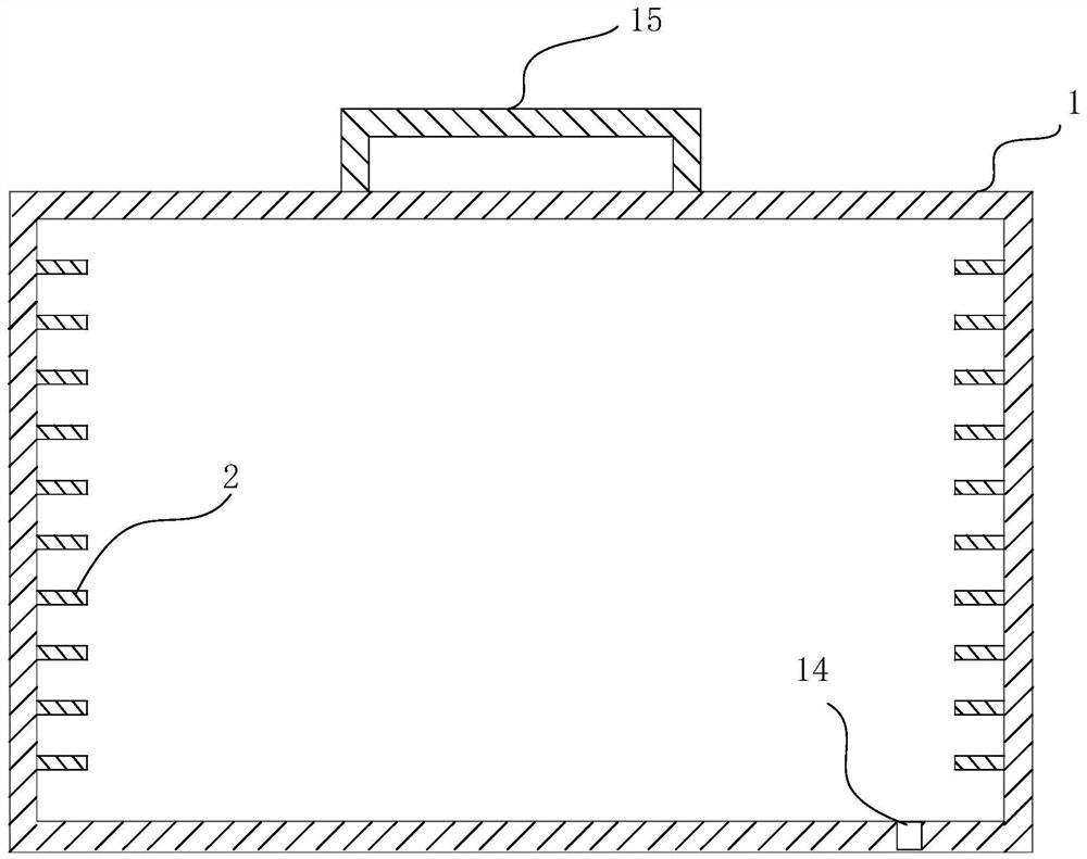
[0077] Such as Figure 4 As shown, in this embodiment, the sensor 3 is a quality sensor 31 for measuring the quality of the wafer. First, a maximum weight threshold and a minimum weight threshold matching the process performed by the machine are input through the input unit 5 . The threshold range=[minimum weight threshold, maximum weight threshold]. When a wafer 7 is processed, the wafer loading and unloading machine 63 opens the door of the wafer cassette body 1, and the wafer 7 is transferred to the carrier bar 2 in the wafer cassette body, and the wafer loading and unloading machine 63 closes the wafer cassette. The opening of the main body 1 is weighed by at least three mass sensors 31 arranged on the carrying bar 2 . The weighing result of each mass sensor 31 will be displayed on the outer surface of the wafer cassette body through the display unit 61 . Normally, the weighing result of each mass sensor 31 is one-third of the mass of the wafer 7 . When there is a weig...
Embodiment 2
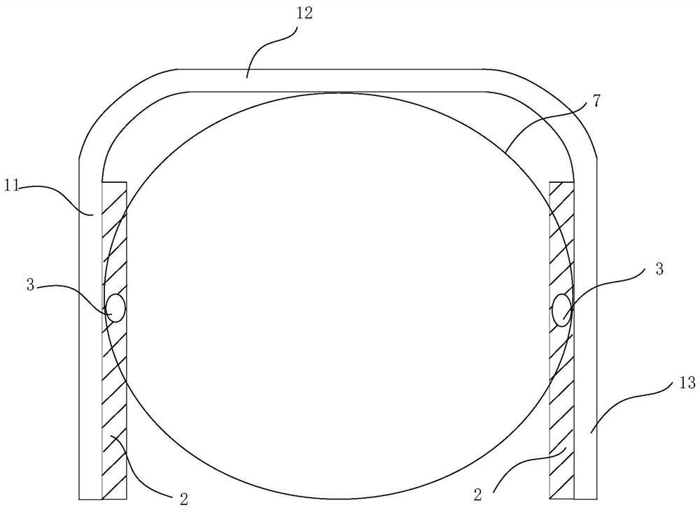
[0080] In this embodiment, the weight of the wafer 7 is still used to determine whether the wafer 7 has defects. Such as Figure 5 As shown, the sensor 3 used in this embodiment is a displacement sensor 32, the wafer 7 is supported by the displacement sensor 32, and a corresponding deformation value is generated according to the elastic deformation of the weight of the wafer 7; the judging unit 4 is based on the elastic deformation The degree to obtain the weight of the wafer 7 .
[0081] Such as Image 6 As shown, the bottom of the displacement sensor 32 can be adjusted up and down, so that the top of the displacement sensor 32 disposed on the same carrier bar is at the same level, and the weighing value of the wafer 7 can be obtained more accurately.
Embodiment 3
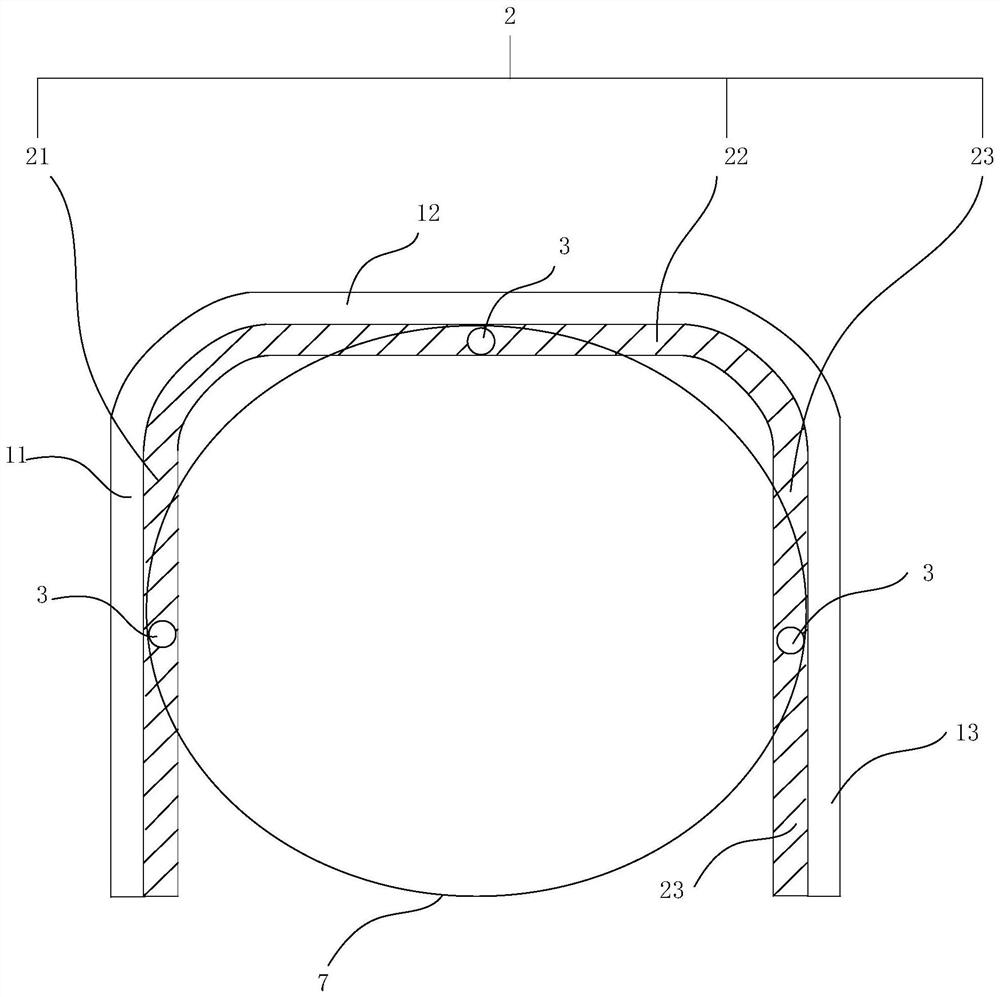
[0083] In this embodiment, whether there is a defect is judged by detecting the thickness of the wafer 7 . The sensor 3 used in this embodiment is a photosensitive sensor 33 . Such as Figure 7 , Figure 8 As shown, the photosensitive sensor 33 is arranged between two vertically adjacent carrying bars 2 . The photosensitive sensor 33 includes an emitting portion 331 and a carrying portion 332 . The carrier part 332 is used to place the wafer, and it is arranged on the top surface of the lower carrier bar 2 among the two adjacent carrier bars 2 up and down; the carrier part 332 can be adjusted up and down so that it is arranged on the same carrier bar. The top ends of the carrying parts 332 of 2 are located on the same horizontal plane; the launching part 331 is arranged on the bottom surface of the upper carrying bar 2 among the two adjacent carrying bars 2 up and down; the launching part 331 emits to the wafer 7 below it. light beam, and generate a distance value accordin...
PUM
 Abstract
Description
Claims
Application Information
 - R&D
- Intellectual Property
- Life Sciences
- Materials
- Tech Scout
- Unparalleled Data Quality
- Higher Quality Content
- 60% Fewer Hallucinations
Browse by: Latest US Patents, China's latest patents, Technical Efficacy Thesaurus, Application Domain, Technology Topic, Popular Technical Reports.
© 2025 PatSnap. All rights reserved.Legal|Privacy policy|Modern Slavery Act Transparency Statement|Sitemap|About US| Contact US: help@patsnap.com