Array substrate, preparation method thereof and display panel

A technology of array substrates and metal layers, which is applied in semiconductor/solid-state device manufacturing, instruments, electrical components, etc., can solve the problems of width-to-length ratio limitation and inflexible adjustment, and achieve the effect of adjusting characteristics and flexible characteristics

Active Publication Date: 2022-03-08
WUHAN CHINA STAR OPTOELECTRONICS SEMICON DISPLAY TECH CO LTD
View PDF5 Cites 0 Cited by
  • Summary
  • Abstract
  • Description
  • Claims
  • Application Information

AI Technical Summary

Problems solved by technology

[0004] An embodiment of the present invention provides an array substrate, which is used to solve the technical problem that the width-to-length ratio of the channel of the active layer of the TFT of the array substrate in the prior art is limited by the process line width and wiring, and cannot be flexibly adjusted.

Method used


Image

  • Array substrate, preparation method thereof and display panel
  • Array substrate, preparation method thereof and display panel
  • Array substrate, preparation method thereof and display panel

Examples


Embodiment Construction

[0035] The following will clearly and completely describe the technical solutions in the embodiments of the present invention with reference to the drawings in the embodiments of the present invention. In the drawings, for clarity and ease of understanding and description, the size and thickness of the components shown in the drawings are not in scale.

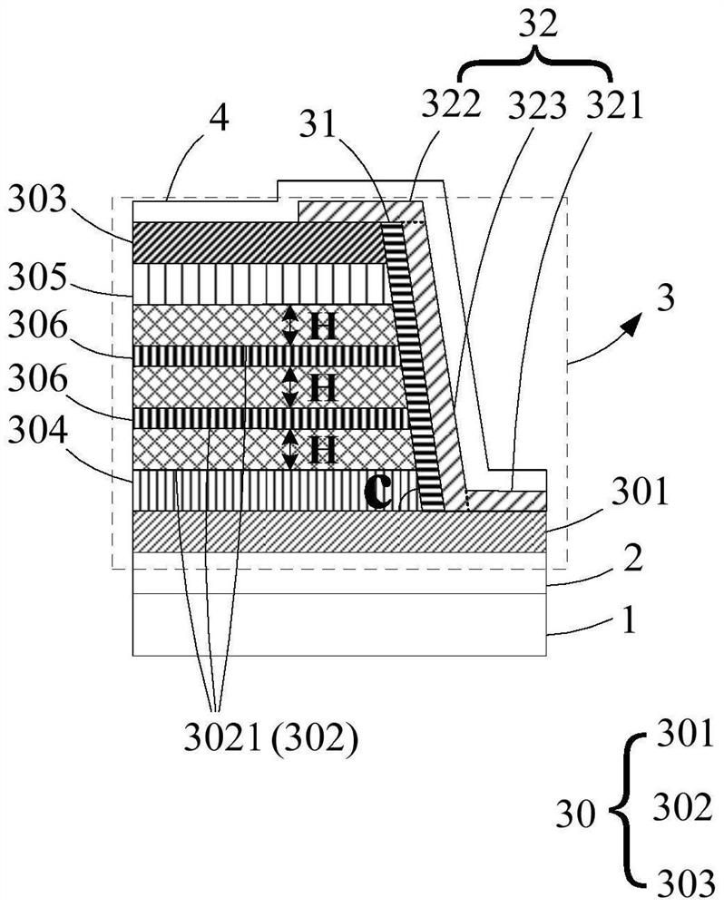
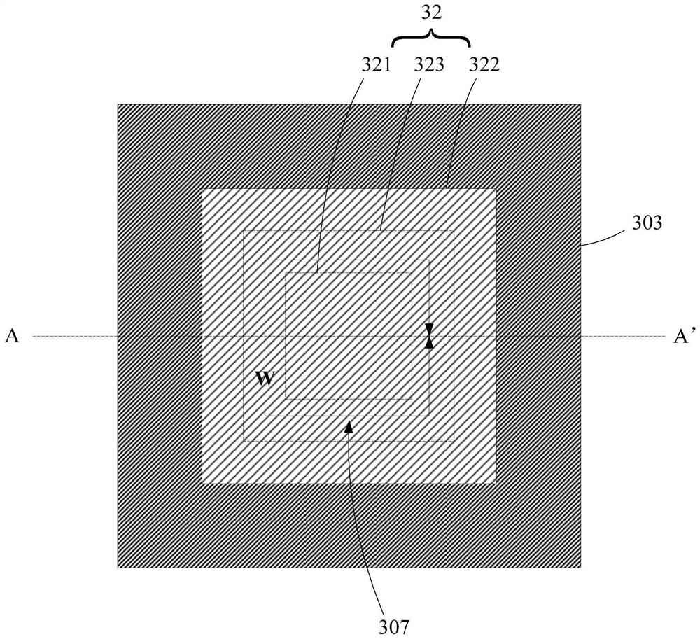
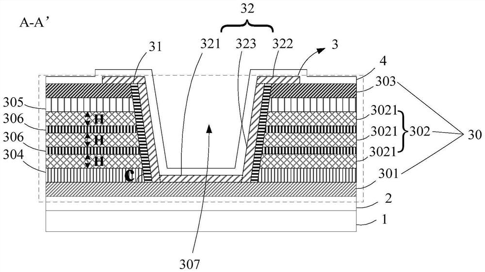
[0036] Such as figure 1As shown, it is a schematic diagram of the basic structure of the array substrate provided by the embodiment of the present invention. The array substrate includes a substrate layer 1 and at least one thin film transistor 3 located on the substrate layer 1; wherein, the thin film transistor 3 includes an electrode layer 30, a gate insulating layer 31, and an active layer 32; the electrode layer 30 includes a stacked first metal layer 301, a second metal layer 302, and a third metal layer 303, and the second metal layer 302 is respectively connected to The first metal layer 301 and the third metal layer ...


PUM

PropertyMeasurementUnit
angleaaaaaaaaaa
thicknessaaaaaaaaaa
thicknessaaaaaaaaaa

Abstract

The invention provides an array substrate and a preparation method thereof and a display panel, the array substrate comprises an electrode layer, a gate insulation layer and an active layer, the electrode layer comprises a first metal layer, a second metal layer and a third metal layer which are stacked, a first end of the active layer is electrically connected with the first metal layer, and a second end of the active layer is electrically connected with the third metal layer. The second end of the active layer is electrically connected with the third metal layer, the second metal layer comprises at least two stacked metal sub-layers in the direction from the first metal layer to the third metal layer, and every two adjacent metal sub-layers are arranged in an insulated mode; according to the invention, the first metal layer, the second metal layer and the third metal layer which form the electrode layer are stacked, the channel of the active layer is arranged on the side wall of the electrode layer, the second metal layer is divided into a plurality of metal sub-layers which are stacked, and the thickness and the number of the metal sub-layers can be regulated and controlled, so that the thickness and the number of the metal sub-layers can be regulated and controlled. Therefore, the width-to-length ratio of the channel of the active layer can be regulated and controlled, and the purpose of flexibly regulating the characteristics of the thin film transistor is achieved.

Description

technical field [0001] The present invention relates to the field of display technology, in particular to an array substrate, a preparation method thereof, and a display panel. Background technique [0002] In recent years, the application of TFT (Thin Film Transistor, thin film transistor) in LCD (Liquid Crystal Display, liquid crystal display) and OLED (Organic Light Emitting Diode, organic light emitting diode) display devices has attracted extensive attention. The active layer semiconductor material used for TFT has undergone a transition from silicon-based to oxide, and the performance of TFT is also continuously improving. [0003] In the traditional process, the width-to-length ratio (W / L) of the channel of the active layer of the TFT is limited by the process line width and wiring, and cannot be adjusted flexibly, which limits the influence of the width-to-length ratio (W / L) on the TFT characteristics. adjustment. Therefore, it is necessary to improve this defect. ...

Claims


Application Information

Patent Timeline
Patent Type & Authority Applications(China)
IPC IPC(8): H01L27/12H01L21/84G09F9/33G09F9/35
CPCH01L27/1222H01L27/124H01L27/127G09F9/33G09F9/35
Inventor 沈海燕黄灿鲜于文旭张春鹏
Owner WUHAN CHINA STAR OPTOELECTRONICS SEMICON DISPLAY TECH CO LTD
Why Eureka
Try Eureka