Array substrate and display panel
A technology for array substrates and display areas, applied in static indicators, nonlinear optics, instruments, etc., can solve problems such as irreversible phase transitions, achieve the effects of improving liquid crystal phase transitions and reducing wiring resistance
- Summary
- Abstract
- Description
- Claims
- Application Information
AI Technical Summary
Problems solved by technology
Method used
Image
Examples
Embodiment 1
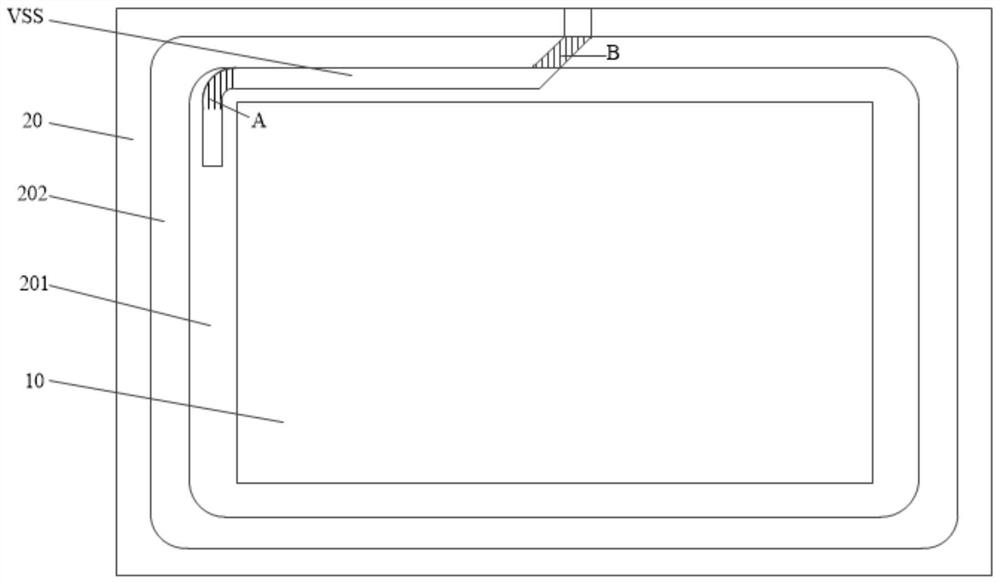
[0030] refer to figure 1 , figure 1 It is a schematic top view of the array substrate of the present application. In this embodiment, the non-display area 20 includes: a sealant area 202 surrounding the display area 10, and an overlapping area B is provided in the sealant area 202, and the overlapping Area B is used for the power signal line VSS to pass through the sealant area 202 .
[0031] It should be noted that all liquid crystal display screens need to use frame glue around the circumference. Through the frame glue curing, the thin film transistor glass substrate and the color filter glass substrate are aligned and fixed, and at the same time, the liquid crystal is sealed between the thin film transistor glass substrate and the color filter glass substrate. in the middle of a glass substrate. Frame glue curing needs to use ultraviolet light irradiation, such as figure 1 As shown, the power signal line VSS must pass through the area where the sealant is located (overla...
Embodiment 2
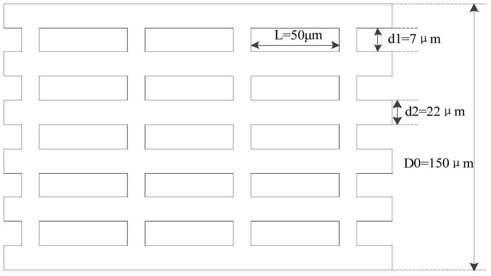
[0043] Based on the above embodiment, the power signal line VSS further includes a hollowed-out wiring in the overlapping area B that has been hollowed out.
[0044] It can be understood that the power signal line VSS adopts a hollow-out process technology, and the power signal line VSS is hollowed out in the overlapping area B.
[0045] The proportion of the hollow area of the hollow line to the area of the overlapping region B is less than or equal to a first preset value, and the proportion is greater than or equal to a second preset value, and the first preset value is greater than the second preset value.
[0046] It is easy to understand that, according to the length L of the hollowed out line, the bus width D0 of the hollowed out line, the width d1 of the hollowed out line, and the width d2 of the non-hollowed out line, the ratio of the area of the hollowed out area to the area of the overlapping area B can be calculated. By adjusting the The size of the line h...
Embodiment 3
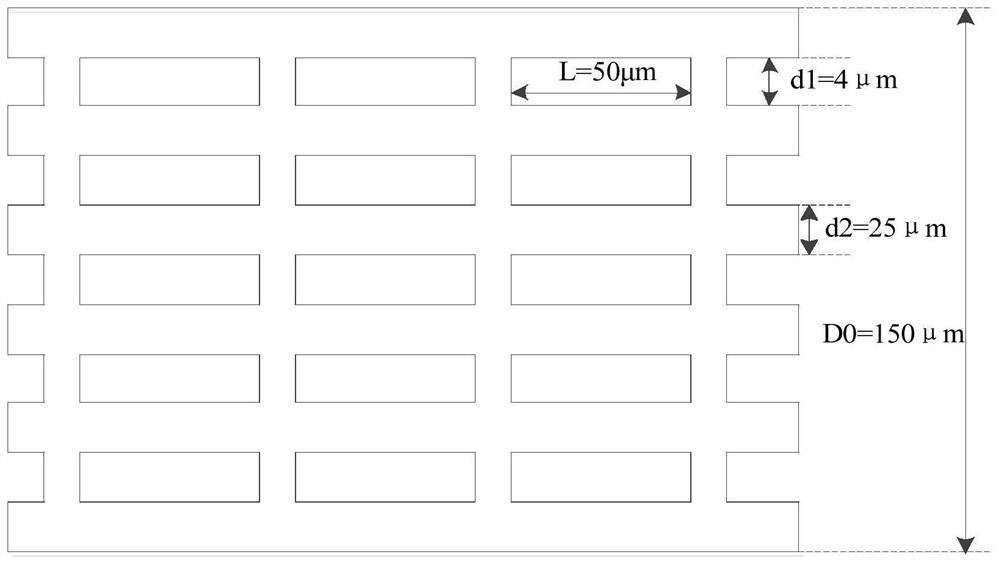
[0053] Based on the above embodiment, the power signal line VSS further includes a hollowed-out wiring in the overlapping area B that has been hollowed out.
[0054] It can be understood that the power signal line VSS adopts a hollow-out process technology, and the power signal line VSS is hollowed out in the overlapping area B.
[0055] The proportion of the hollow area of the hollow line to the area of the overlapping region B is less than or equal to a first preset value, and the proportion is greater than or equal to a second preset value, and the first preset value is greater than the second preset value.
[0056] It is easy to understand that, according to the length L of the hollowed out line, the bus width D0 of the hollowed out line, the width d1 of the hollowed out line, and the width d2 of the non-hollowed out line, the ratio of the area of the hollowed out area to the area of the overlapping area B can be calculated. By adjusting the The size of the line h...
PUM
 Abstract
Description
Claims
Application Information


