

Method for sealing wafer by using carrier plate
A technology of wafers and discs, which is applied in the field of sealing wafers with discs, can solve the problems of not meeting the requirements of wafer high-temperature process, poor high-temperature resistance of adhesives, material limitations, etc., to prevent movement or falling, Low production cost and the effect of overcoming temperature limitations
- Summary
- Abstract
- Description
- Claims
- Application Information
AI Technical Summary
Problems solved by technology
Method used
Image

Examples
Embodiment 1
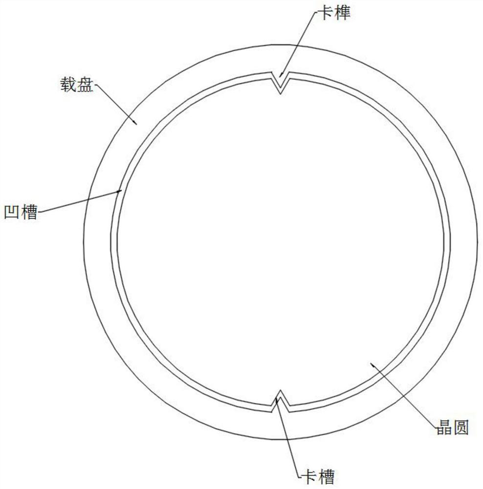
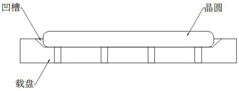
[0031] Such as Figure 1-4 As shown, a method for sealing a wafer by using a carrier plate, the surface of the carrier plate is provided with a groove, and the inner wall of the groove is symmetrically provided with tenons, and the method for sealing the wafer includes the following steps:
[0032] S1. Open a groove symmetrically on the edge of the wafer to be processed by etching or mechanical grinding, and then put the wafer into the groove on the surface of the carrier, and the groove is matched with the tenon;
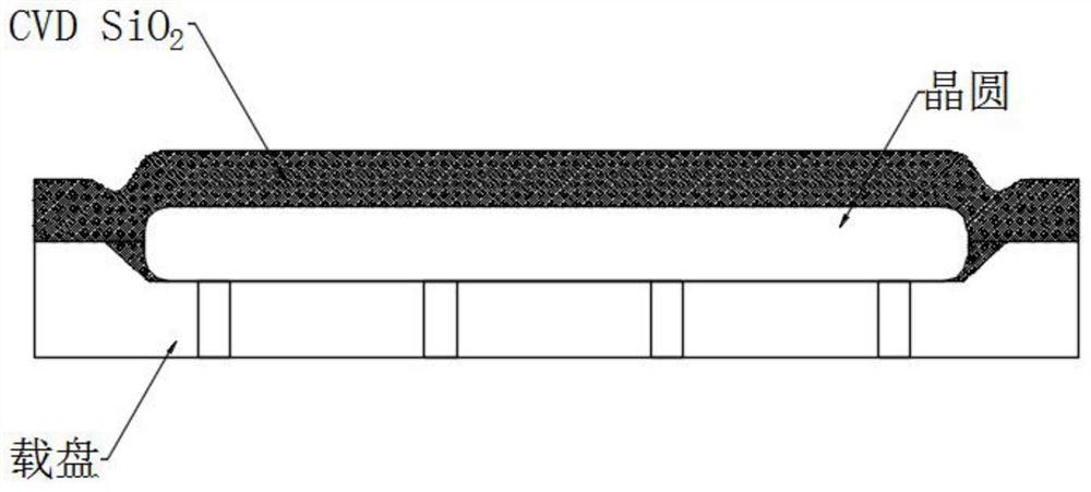
[0033] S2. Deposit SiO on the surface of the wafer and the carrier plate by CVD 2 blocking layer;
[0034] S3. Grinding SiO by CMP 2 Plug the layer to the wafer surface to planarize the wafer surface;
[0035] S4. After the front process of the wafer is completed, SiO is removed by plasma etching 2 After the plugging layer is removed, the wafer can be released and taken out for subsequent processes.
Embodiment 2
[0037] Such as Figure 5-7 As shown, a method for sealing a wafer by using a carrier plate, the surface of the carrier plate is provided with a groove, and the inner wall of the groove is symmetrically provided with tenons, and the method for sealing the wafer includes the following steps:
[0038] S1. Open a groove symmetrically on the edge of the wafer to be processed by etching or mechanical grinding, and then put the wafer into the groove on the surface of the carrier, and the groove is matched with the tenon;
[0039] S2, forming an SOG blocking layer after spin-coating on the surface of the wafer and the carrier plate;
[0040] S3, grinding the SOG plugging layer to the wafer surface by CMP, so that the wafer surface is planarized;
[0041] S4. After the front-side process of the wafer is completed, the SOG blocking layer is removed by plasma etching, and the wafer can be released and taken out for subsequent process.
Embodiment 3
[0043] Such as Figure 8-10 As shown, a method for sealing a wafer by using a carrier plate, the surface of the carrier plate is provided with a groove, and the inner wall of the groove is symmetrically provided with tenons, and the method for sealing the wafer includes the following steps:
[0044] S1. Open a groove symmetrically on the edge of the wafer to be processed by etching or mechanical grinding, and then put the wafer into the groove on the surface of the carrier, and the groove is matched with the tenon;
[0045] S2, coating the surface of the wafer and the carrier plate with polyimide and curing to form a blocking layer;
[0046] S3. Grinding the polyimide plugging layer to the wafer surface by CMP to planarize the wafer surface;
[0047] S4. After the front-side process of the wafer is completed, the plugging layer is removed by dissolving with an organic solvent, and the wafer can be released and taken out for subsequent process.
[0048] Such as Figure 11 As...
PUM
 Abstract
Description
Claims
Application Information