Semiconductor structure and forming method of semiconductor structure

A semiconductor and gate structure technology, which is applied in semiconductor devices, semiconductor/solid-state device manufacturing, semiconductor/solid-state device components, etc., can solve problems such as metal gate isolation, reduce damage and improve performance

Pending Publication Date: 2022-03-18
SEMICON MFG INT (SHANGHAI) CORP +1
View PDF0 Cites 0 Cited by
  • Summary
  • Abstract
  • Description
  • Claims
  • Application Information

AI Technical Summary

Problems solved by technology

[0003] However, after forming the metal gate, there are still some challenges in how to effectively isolate the metal gate

Method used


Image

  • Semiconductor structure and forming method of semiconductor structure
  • Semiconductor structure and forming method of semiconductor structure
  • Semiconductor structure and forming method of semiconductor structure

Examples


Embodiment Construction

[0034] As mentioned in the background, there are still many challenges in the manufacturing process of the metal gate at the current stage. Now analyze and illustrate in conjunction with specific embodiment.

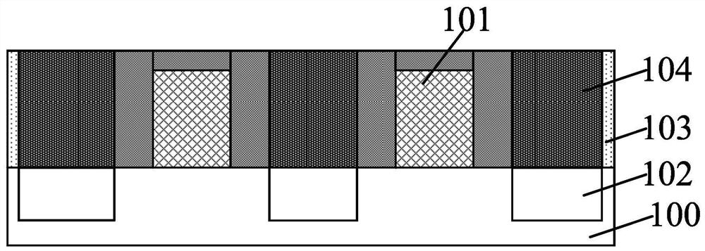
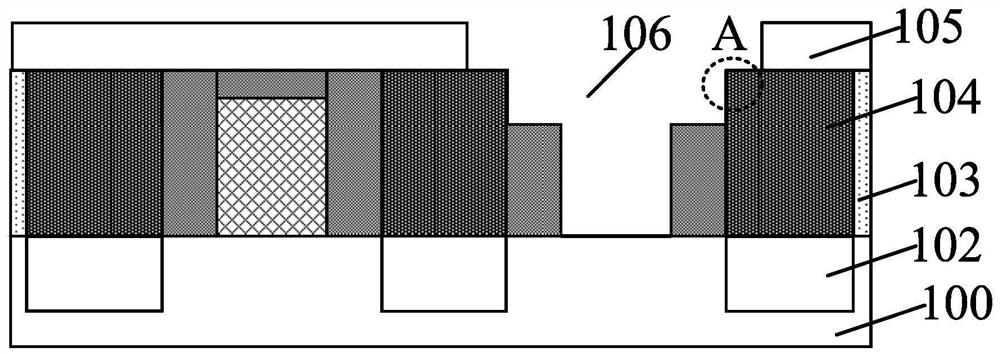
[0035] figure 1 and figure 2 It is a schematic cross-sectional structure diagram of the formation process of the semiconductor structure in an embodiment.

[0036] Please refer to figure 1 , providing a substrate 100; on the substrate 100, a plurality of gate structures 101 arranged in parallel are formed, the side walls of the gate structures 101 have sidewalls (not marked), and the top of the gate structure 101 has a barrier layer (not marked ); forming a source-drain doped region 102 in the substrate on both sides of the gate structure 101; forming a dielectric layer 103 on the substrate 100, and the dielectric layer 103 is located on the sidewall of the gate structure 101; removing the source-drain doped region Dielectric layer 103 on 102 , an opening (not shown...


PUM


Abstract

The invention discloses a semiconductor structure and a forming method of the semiconductor structure. The gate structures are arranged on the substrate in parallel; the source-drain doped regions are positioned in the substrate at two sides of each gate structure; the side wall structure is located on the partial side wall of the gate structure, and the top surface of the side wall structure is lower than the top surface of the gate structure; the conducting layer is located on the source-drain doped region, and the conducting layer and the gate structure are isolated by a side wall structure; and the barrier layer is positioned on the conductive layer and the side wall structure. The barrier layer and the side wall structure in the semiconductor structure can jointly protect the top surface and the side wall surface of the conductive layer, and damage to the conductive layer is reduced.

Description

technical field [0001] The invention relates to the field of semiconductor manufacturing, in particular to a semiconductor structure and a method for forming the semiconductor structure. Background technique [0002] The semiconductor integrated circuit (IC) industry has experienced exponential growth. In the course of IC evolution, functional density (ie, the number of interconnected devices per chip area) has generally increased, while geometry size (ie, the smallest component or line that can be produced using a fabrication process) has decreased. As technology nodes shrink, metal gates are used to replace typical polysilicon gates to improve device performance. One process for forming the metal gate is known as a replacement gate or "gate last" process. [0003] However, there are still some challenges in how to effectively isolate the metal gate after the metal gate is formed. Contents of the invention [0004] The technical problem solved by the present invention ...

Claims


Application Information

Patent Timeline
Patent Type & Authority Applications(China)
IPC IPC(8): H01L27/088H01L23/528H01L21/8234H01L21/768
CPCH01L27/088H01L23/5283H01L21/76895H01L21/823475H01L21/823468
Inventor 陈卓凡
Owner SEMICON MFG INT (SHANGHAI) CORP
Why Eureka
Try Eureka