Design method of broadband radio frequency lossless matching network chip of laser chip

A matching network and chip design technology, applied in lasers, devices for controlling laser output parameters, semiconductor lasers, etc., can solve the problems of RF chip-to-laser chip loss link noise, high RF signal noise coefficient, impedance mismatch, etc. Achieve the effect of improving system sensitivity, low noise figure and reducing reflection

Active Publication Date: 2022-03-22
SOUTHWEST CHINA RES INST OF ELECTRONICS EQUIP
View PDF3 Cites 0 Cited by
  • Summary
  • Abstract
  • Description
  • Claims
  • Application Information

AI Technical Summary

Problems solved by technology

Compared with traditional microwave technology, microwave photonic technology has many advantages, but the noise figure introduced during the interconversion process of radio frequency signals and optical signals is relatively large, which becomes a key factor affecting the dynamic range of the system in the system
[0003] Especially in the serious impedance mismatch between the RF chip and the laser chip, the lossy matching method of series resistance is adopted in the industry, which leads to obvious loss in the transmission process from the RF chip to the laser chip and causes the link noise to increase
The impedance matching between the RF chip and the laser chip is realized by using a lossless matching method, which greatly reduces the noise figure of the microwave photonic link. However, the input and output signals of the laser chip are in the form of radio frequency signals and optical signals, and the traditional method of microwave parameter extraction Difficult to apply to microwave photonic systems

Method used


Image

  • Design method of broadband radio frequency lossless matching network chip of laser chip
  • Design method of broadband radio frequency lossless matching network chip of laser chip
  • Design method of broadband radio frequency lossless matching network chip of laser chip

Examples


Embodiment Construction

[0028] The present invention will be further described below in conjunction with the accompanying drawings.

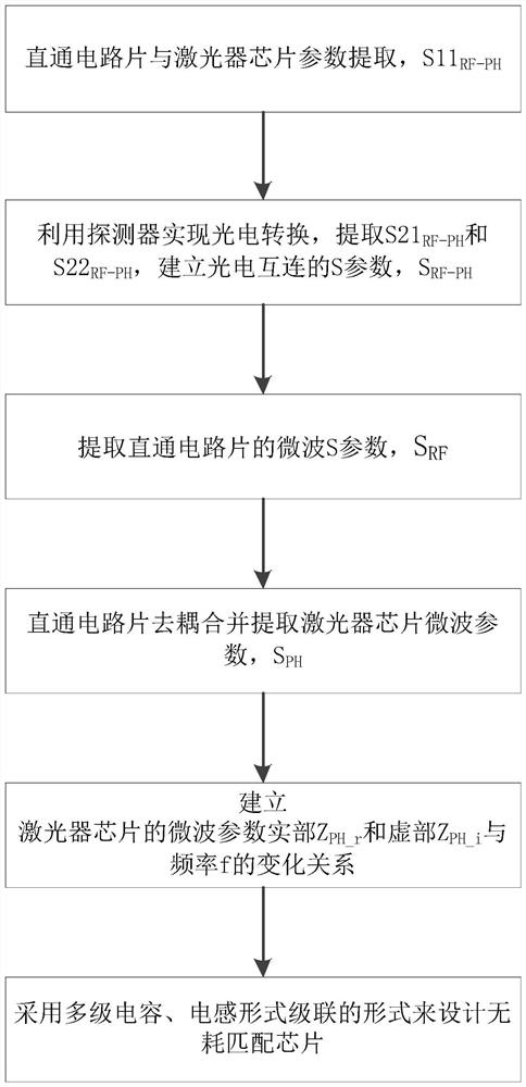
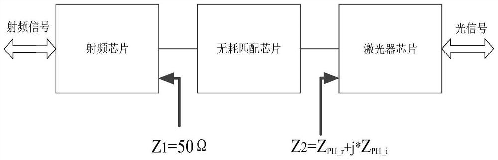
[0029] The invention proposes a design method for a broadband radio frequency lossless matching network chip of a laser chip. By extracting the microwave parameters of the laser chip, a numerical fitting method is used to simulate the change curve of the port impedance of the laser chip with the frequency of the received radio frequency signal, thereby designing the radio frequency The matching network chip between the chip and the laser chip realizes the lossless impedance matching between the radio frequency chip and the laser chip. The specific plan is as follows:

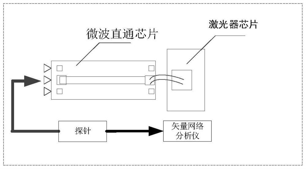
[0030] Step 1, electrically interconnecting the microwave through chip and the laser chip, and extracting the input reflection component of the microwave S-parameter of the interconnected microwave through chip and the laser chip;

[0031] Step 2. Couple the optical signal output by the laser chip after...


PUM


Abstract

The invention provides a design method for a broadband radio frequency lossless matching network chip of a laser chip. The design method comprises the following steps: step 1, extracting an input reflection component of a microwave S parameter of a microwave straight-through chip and a laser chip which are connected with each other; 2, optical signals output by the laser chips after electrical interconnection are coupled to a detector, and microwave S parameters of electro-optical interconnection of the laser chips and the microwave straight-through chips are obtained by combining input reflection components; step 3, extracting a microwave S parameter of the microwave straight-through chip; step 4, calculating a microwave S parameter of the laser chip by adopting a de-embedding mode; step 5, acquiring an impedance parameter of the laser chip according to the microwave S parameter of the laser chip; and step 6, designing a matching network chip according to the impedance parameter of the laser chip. According to the invention, good impedance matching between the laser chip and the radio frequency chip can be realized, the signal transmission quality and the system sensitivity are improved, and the device can be widely applied to various microwave photon integrated products.

Description

technical field [0001] The invention relates to the field of microwave photon signals, in particular to a design method for a broadband radio frequency lossless matching network chip of a laser chip. Background technique [0002] As an interdisciplinary subject combining photon technology and microwave technology, microwave photonics transforms radio frequency microwave signals into the optical domain, and uses optical methods to realize the transmission, generation, distribution, and processing of radio frequency signals. Compared with traditional microwave technology, microwave photonics has a series of advantages such as broadband, high speed, parallelism, compactness, electromagnetic compatibility and anti-interference. Compared with traditional microwave technology, microwave photonic technology has many advantages, but the noise figure introduced during the interconversion process of radio frequency signals and optical signals is relatively large, which becomes a key f...

Claims


Application Information

Patent Timeline
Patent Type & Authority Applications(China)
IPC IPC(8): H04B10/2575H04B10/50H01S5/06
CPCH04B10/25752H04B10/503H01S5/0607Y02D30/70
Inventor 吕晓萌赵炳旭廖翱张继帆伍艺龙卢子焱许玮华李希斌
Owner SOUTHWEST CHINA RES INST OF ELECTRONICS EQUIP
Why Eureka
Try Eureka