Supercharge Your Innovation With Domain-Expert AI Agents!

High-gain and high-efficiency on-chip antenna based on silicon-based process

An on-chip antenna, high-gain technology, applied in the directions of separately powered antenna arrays, antennas, antenna coupling, etc., can solve the problems of different substrates, large differences in antenna radiation performance, and insignificant improvement of on-chip antenna gain and efficiency. , to achieve the effect of large bandwidth, good shielding effect and gain improvement

Inactive Publication Date: 2022-03-25
ZHEJIANG LAB
View PDF6 Cites 0 Cited by
  • Summary
  • Abstract
  • Description
  • Claims
  • Application Information

AI Technical Summary

Problems solved by technology

Although the antennas reported above have a simple structure and can achieve multiple functions such as dual-frequency and dual-polarization, the main difference between the on-chip antenna and the PCB antenna is that the substrates used are different, resulting in a large difference in the radiation performance of the antenna. The reported on-chip antennas are not obvious in terms of gain and efficiency improvement, so the current difficulties that need to be solved for silicon-on-chip antennas still focus on the improvement of gain and efficiency.

Method used


Image

  • High-gain and high-efficiency on-chip antenna based on silicon-based process
  • High-gain and high-efficiency on-chip antenna based on silicon-based process
  • High-gain and high-efficiency on-chip antenna based on silicon-based process

Examples


Embodiment Construction

[0032] In order to make the object, technical solution and advantages of the present invention clearer, the present invention will be further described in detail below with reference to the accompanying drawings and embodiments. However, it should be understood that the specific embodiments described here are only used to explain the present invention, and are not intended to limit the scope of the present invention. Also, in the following description, descriptions of well-known structures and techniques are omitted to avoid unnecessarily obscuring the concept of the present invention.

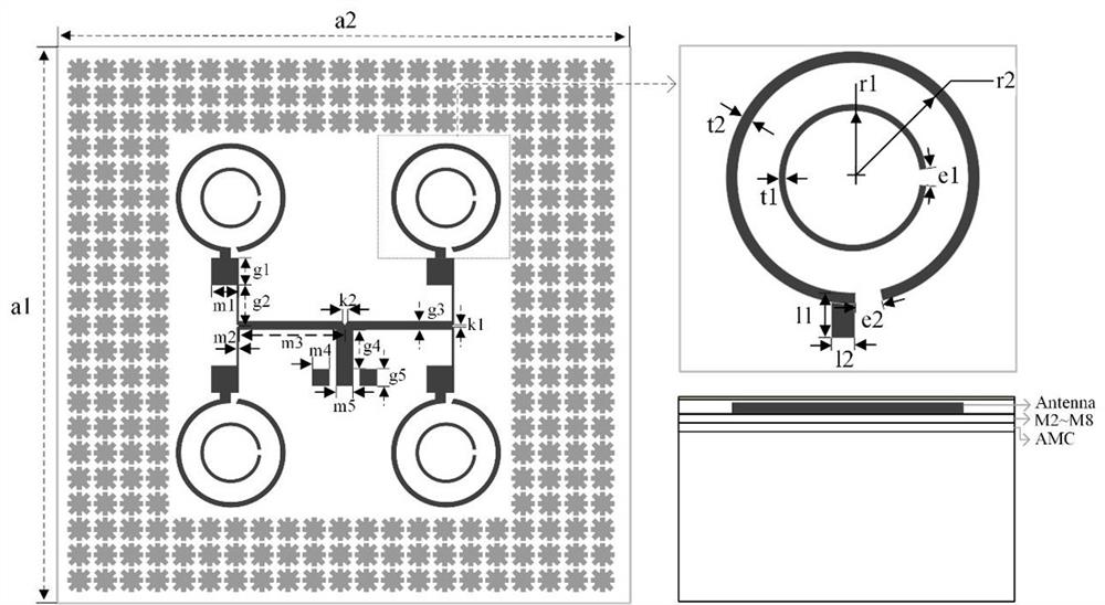
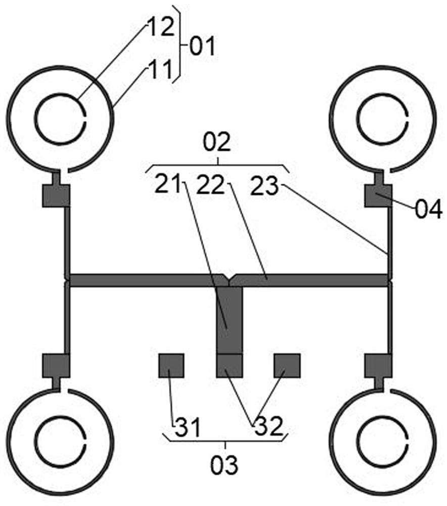
[0033] like Figure 1-3 As shown, the embodiment of the present invention provides a high-gain and high-efficiency on-chip antenna of a silicon-based process, including a silicon substrate, and M1 to M9 metal layers are arranged on the silicon substrate, and two rows of metal layers are arranged on the M9 metal layer. Two columns of array antennas, the array antenna includes four loop antenna...


PUM


Abstract

The invention discloses a high-gain and high-efficiency on-chip antenna of a silicon-based process, which comprises a silicon substrate, nine metal layers are sequentially arranged on the silicon substrate, two rows and two columns of array antennas are arranged on the ninth metal layer, each array antenna comprises four loop antenna units, a T-shaped power divider and a coplanar waveguide feed end, the four annular antenna units are connected with the coplanar waveguide feed end through the T-shaped power divider, each annular antenna unit comprises an outer opening resonance ring and an inner opening resonance ring which are coaxially arranged, and an artificial magnetic conductor layer is arranged on a first metal layer below the array antenna. The invention provides a high-gain and high-efficiency on-chip antenna of a silicon-based process. The high-gain and high-efficiency on-chip antenna comprises a two-row and two-column array antenna located on an M9 layer and an artificial magnetic conductor layer located on an M1 layer, the artificial magnetic conductor layer has the same-direction reflection characteristic, the reflection phase at 60 GHz is 0 degree, the in-phase reflection phase band gap is 53.1 GHz-67.7 GHz, and the license-free bandwidth range near 60 GHz is completely covered.

Description

technical field [0001] The invention relates to the technical fields of antenna design and wireless communication, in particular to a high-gain and high-efficiency on-chip antenna of a silicon-based process. Background technique [0002] With the rapid development of wireless communication technology, the iterative cycles of smart homes, smartphones, and wireless wearable devices are getting shorter and shorter. At the same time, the requirements for wireless communication transmission technology are getting higher and higher. Gbps wireless transmission technology will become the future wireless The mainstream of communication technology. In 2001, the Federal Communications Commission (FCC) released the 57GHz to 64GHz license-free spectrum. Compared with other frequency bands, the 60GHz license-free spectrum has the advantages of large bandwidth, strong anti-interference ability, and high transmission rate. [0003] The development and application of high-frequency bands al...

Claims


Application Information

Patent Timeline
Patent Type & Authority Applications(China)
IPC IPC(8): H01Q1/22H01Q1/38H01Q1/48H01Q1/50H01Q1/52H01Q7/00H01Q19/10H01Q21/00H01Q21/06
CPCH01Q1/38H01Q7/00H01Q1/2283H01Q1/50H01Q1/526H01Q19/104H01Q21/061H01Q21/0006H01Q21/0075H01Q1/48
Inventor 靳书珍陈娜渠慎奇钱程玉虓
Owner ZHEJIANG LAB
Features
  • R&D
  • Intellectual Property
  • Life Sciences
  • Materials
  • Tech Scout
  • Unparalleled Data Quality
  • Higher Quality Content
  • 60% Fewer Hallucinations
Learn More