
SIW transmission line capable of loading direct-current electric field bias

A DC electric field and transmission line technology, applied in the microwave field, can solve the problems of high loss, low Q value, and the guiding wave structure cannot be loaded with DC electric field bias, etc., and achieves the effect of low loss and reduction of radiation loss.

Active Publication Date: 2022-04-05
UNIV OF ELECTRONIC SCI & TECH OF CHINA
View PDF5 Cites 0 Cited by
  • Summary
  • Abstract
  • Description
  • Claims
  • Application Information

AI Technical Summary

Problems solved by technology

[0004] In view of the above existing problems or deficiencies, in order to solve the problem that the existing waveguide structure cannot be loaded with DC electric field bias, or loaded on transmission line structures such as striplines and coplanar waveguides, there are problems of high loss and low Q value; the present invention provides a The SIW transmission line that can be loaded with a DC electric field bias can reduce the radiation loss of the SIW by improving the metal through hole as the DC blocking structure designed in the present invention on the basis of the substrate integrated waveguide structure, and adding a row of the above DC blocking structures. Realize the function of isolating DC electric field under low loss

Method used


Image

  • SIW transmission line capable of loading direct-current electric field bias
  • SIW transmission line capable of loading direct-current electric field bias
  • SIW transmission line capable of loading direct-current electric field bias

Examples


Embodiment Construction

[0030] The present invention will be further described in detail below with reference to the accompanying drawings and a specific embodiment applied to the X-band.

[0031] A design method for an X-band loadable DC electric field biased SIW transmission line, comprising the following steps:

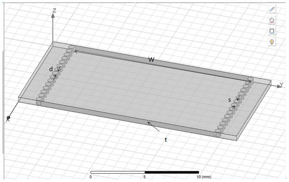
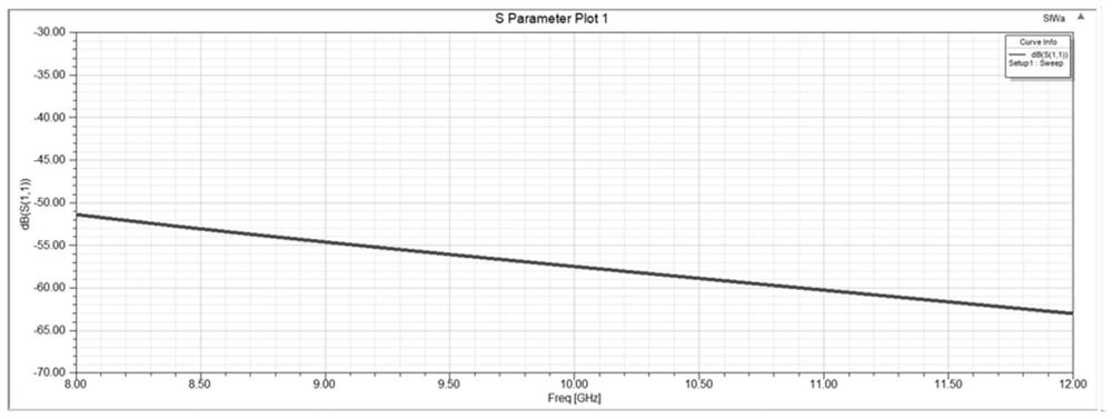
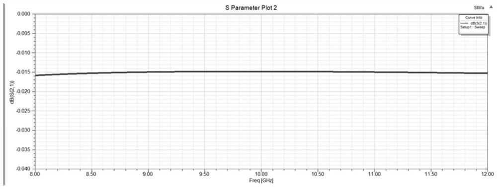
[0032] Step 1. According to the equivalent formula of the substrate-integrated waveguide and the traditional rectangular waveguide, the substrate-integrated waveguide is designed under the condition of satisfying the radiation loss, and the polytetrafluoroethylene material is selected as the medium, and the thickness of the dielectric substrate is t=0.80mm. Electrical constant ε r =2.1, determine the width w=17.5mm of the substrate-integrated waveguide, the diameter of the metallized through-hole d=0.4mm and the distance between the centers of the through-holes s=0.45mm; model and analyze the transmission performance of the substrate-integrated waveguide in HFSS, and obtain In the entire...


PUM


Abstract

The invention relates to a microwave technology, in particular to an SIW (substrate integrated waveguide) transmission line capable of loading direct-current electric field bias. On the basis of the substrate integrated waveguide, a metal through hole structure is changed into a blocking structure, a row of inverted and identical blocking structures are additionally arranged to reduce radiation loss, and equivalent capacitance is increased to enable the substrate integrated waveguide to approach transmission performance of a traditional SIW transmission line. The electric schematic diagram of the blocking structure is equivalent to periodically loading a shunt capacitor on the basis of the traditional SIW, so that the capacitance value needs to be increased as much as possible on the premise of meeting the size requirement, namely, the spacing is reduced and the capacitance area is increased. Compared with a single-row structure, the double-row structure has the advantages that radiation loss is reduced, equivalently, a shunt capacitor is additionally arranged, the capacitance value is further increased, and the performance of the whole blocking transmission line is close to that of an SIW (substrate integrated waveguide) transmission line. According to the invention, the function of loading a direct-current bias electric field is met, but the loss is far lower than that of the existing strip line and coplanar waveguide structure.

Description

technical field [0001] The invention relates to microwave technology, in particular to an SIW transmission line capable of loading DC electric field bias. Background technique [0002] With the development and progress of science and technology, microwave technology is gradually developing towards miniaturization and integration. The SIW structure has the advantages of low radiation, low insertion loss, high Q value, high power capacity, miniaturization and easy connection. Ferroelectric materials have the characteristics of changing the dielectric constant of ferroelectric materials by changing the electric field applied to ferroelectric materials, and have many advantages such as high power capacity and fast polarization speed, and can be applied to many microwave devices. designing. [0003] Existing ferroelectric materials are mostly used in structures such as striplines and coplanar waveguides. The loss caused by the transmission line itself is relatively large, and t...

Claims


Application Information

Patent Timeline
IPC IPC(8): H01P3/00H01P11/00
Inventor 汪晓光林铮赵晓琴
Owner UNIV OF ELECTRONIC SCI & TECH OF CHINA
Learn More