Pressure sensor based on FBAR structure and preparation method thereof
A pressure sensor and substrate technology, applied in the field of sensors, can solve problems such as reducing pressure sensitivity, and achieve the effects of small range, fast response speed and high sensitivity
- Summary
- Abstract
- Description
- Claims
- Application Information
AI Technical Summary
Problems solved by technology
Method used
Image
Examples
Embodiment 1
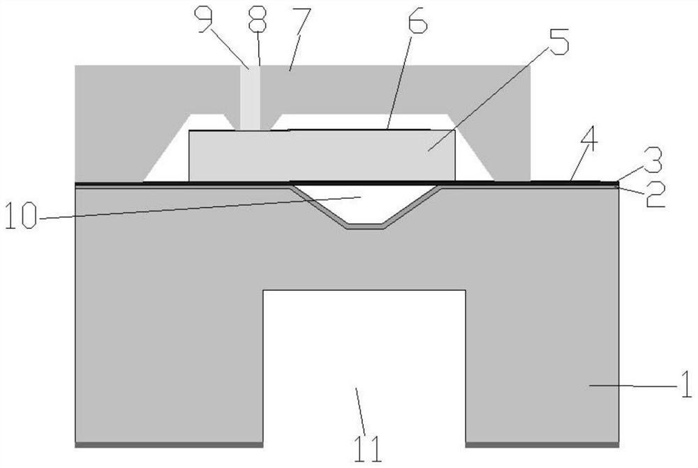
[0059] see figure 1 , in an embodiment of the present invention, a pressure sensor based on an FBAR structure includes a substrate 1, preferably, the substrate is a silicon wafer with a high resistance (100) crystal orientation, and a groove is opened on the top of the substrate 1, and the groove The depth is 1-30 μm, the surface of the substrate 1 is covered with an insulating layer 2, preferably, the insulating layer 2 is made of SiO 2 、Si 3 N 4 etc.; further, the material of the insulating layer 2 is SiO prepared by LPCVD or thermal oxygen oxidation process 2 , the thickness of the insulating layer 2 is 0.3-0.6 μm; the insulating layer 2 and the top groove of the base 1 surround the air chamber 10; the insulating layer 2 is covered with a supporting layer 3, preferably, the supporting layer 3 is made of For the preparation of Si by PECVD or LPCVD 3 N 4 , the supporting layer 3 has a thickness of 0.3-1 μm; the supporting layer 3 is provided with a piezoelectric oscillat...
Embodiment 2
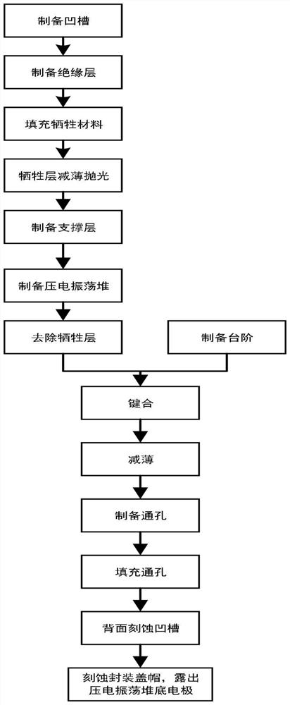
[0063] see Figure 2-19 , on the basis of Example 1, the above-mentioned preparation method of the pressure sensor based on the FBAR structure includes substrate technology, packaging cap technology, substrate and packaging cap bonding, packaging cap thinning, preparing through holes on the packaging cap, filling through holes Preparation of grooves at the bottom of the hole and substrate, and etching of the packaging cap to expose the bottom electrode of the piezoelectric oscillation stack; the substrate process includes preparation of grooves at the top of the substrate, preparation of an insulating layer, filling of sacrificial layer materials, thinning and polishing of the sacrificial layer, and preparation of piezoelectric stacks; packaging The capping process includes preparation steps; specifically, the following steps are included:
[0064] 1) Wet etching a groove on the top of the silicon wafer substrate 1 with a high resistance (100) crystal orientation, with a depth...
PUM
| Property | Measurement | Unit |
|---|---|---|
| Depth | aaaaa | aaaaa |
| Thickness | aaaaa | aaaaa |
| Thickness | aaaaa | aaaaa |
Abstract
Description
Claims
Application Information


