Semiconductor structure and forming method thereof

A semiconductor and active area technology, applied in semiconductor devices, transistors, electrical solid devices, etc., can solve the problem that the performance of flash memory structure needs to be further improved, and achieve the effect of improving short channel effect, reducing leakage and reducing interconnection

Pending Publication Date: 2022-04-12
HUA HONG SEMICON WUXI LTD
View PDF0 Cites 2 Cited by
  • Summary
  • Abstract
  • Description
  • Claims
  • Application Information

AI Technical Summary

Problems solved by technology

[0004] The performance of the existing flash memory structure needs to be further improved

Method used


Image

  • Semiconductor structure and forming method thereof
  • Semiconductor structure and forming method thereof
  • Semiconductor structure and forming method thereof

Examples


Embodiment Construction

[0030] It should be noted that the "surface" and "upper" in this specification are used to describe the relative positional relationship in space, and are not limited to direct contact.

[0031] As mentioned in the background technology, with the continuous shrinking of device structure size, problems such as short channel effect and leakage-induced barrier lowering effect brought about by the shrinking gate width have seriously limited the development of flash memory structure. The existing flash memory structure Technology needs to be further improved.

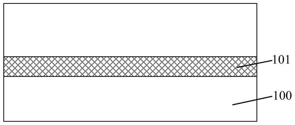
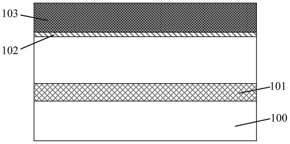
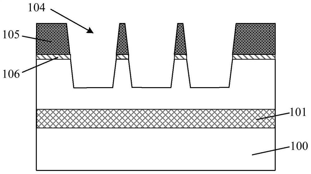
[0032] In order to solve the above problems, the present invention provides a method for forming a semiconductor structure, each of the active regions includes a first region and second regions respectively located on both sides of the first region, the first region and the The second area is arranged along the first direction, and the top surface of the second area is lower than the top surface of the first area, and a numb...


PUM

PropertyMeasurementUnit
thicknessaaaaaaaaaa
thicknessaaaaaaaaaa

Abstract

The invention discloses a semiconductor structure and a forming method thereof. The method comprises the following steps: providing an initial substrate; a substrate and a plurality of active regions located on the substrate and arranged in the first direction are formed, the first direction is parallel to the surface of the substrate, each active region comprises a first region and second regions located on the two sides of the first region respectively, and the first region and the second regions are arranged in the first direction, the top surface of the second region is lower than the top surface of the first region; forming a plurality of floating gates on the surfaces of the plurality of active regions; and forming an isolation layer between the adjacent active regions, wherein the isolation layer is also located on a part of the side wall of the floating gate. The channel width of the formed device is increased, the threshold voltage stability of the device is improved, the influences of the short channel effect and the drain induced barrier reduction effect of the device are improved, and therefore the performance of the device is improved.

Description

technical field [0001] The invention relates to the technical field of semiconductor manufacturing, in particular to a semiconductor structure and a forming method thereof. Background technique [0002] Flash Memory (Flash Memory) is a non-volatile memory, which can keep data for a long time even when there is no current supply, even if the power is turned off, the data will not be lost. Flash memory is mainly divided into two types, NOR and NAND, commonly referred to as NORFlash and NAND Flash. Among them, NOR Flash is also called encoded flash memory. Because of its features such as direct code execution, high reliability, and fast reading speed, it has become the mainstream non-volatile memory in flash memory technology. [0003] At present, the mainstream structure of NOR Flash is ETOX (Erasable Programmable Read Only Memory with Tunnel Oxide, Erasable Programmable Read Only Memory with Tunnel Oxide) structure. In order to achieve faster computing speed, larger data s...

Claims


Application Information

Patent Timeline
Patent Type & Authority Applications(China)
IPC IPC(8): H01L27/11521H01L29/06H01L29/788
Inventor 刘勃彤何应春顾林
Owner HUA HONG SEMICON WUXI LTD
Why Eureka
Try Eureka