LED device

A technology for LED devices and LED chips, applied in semiconductor devices, electrical components, circuits, etc., can solve the problems of reduced reliability of LED devices, easy generation of gaps, failure of LED devices, etc., to improve hydrolysis resistance, increase path distance, The effect of prolonging the service life

Pending Publication Date: 2022-04-12
FOSHAN NATIONSTAR OPTOELECTRONICS CO LTD
View PDF0 Cites 0 Cited by
  • Summary
  • Abstract
  • Description
  • Claims
  • Application Information

AI Technical Summary

Problems solved by technology

During the bonding process of the bonding wire, when the distance between the electrode of the LED chip and the edge of the LED chip is far away, the bonding wire is easy to touch the edge of the LED chip, causing leakage of the LED device and reducing the reliability of the LED device
During the encapsulation adhesive covering process, due to the difference in material properties between the encapsulation adhesive and the stent electrodes, gaps are likely to be formed when the encapsulation adhesive and the stent electrodes are combined. The gap between the packaging glue and the bracket electrode invades into the interior of the LED device, which accelerates the migration of metal ions on the surface of the bracket electrode, causing the LED chip electrode to fall off and disconnect, resulting in LED device failure and reduced reliability of the LED device.

Method used


Image

  • LED device
  • LED device
  • LED device

Examples


Embodiment Construction

[0030] The present invention will be further described in detail below in conjunction with the accompanying drawings and embodiments. It should be understood that the specific embodiments described here are only used to explain the present invention, but not to limit the present invention. In addition, it should be noted that, for the convenience of description, only some structures related to the present invention are shown in the drawings but not all structures.

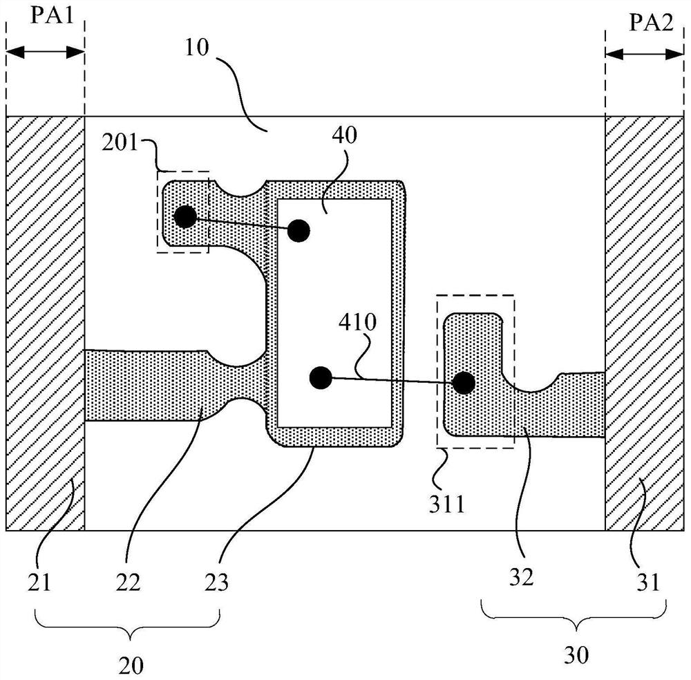
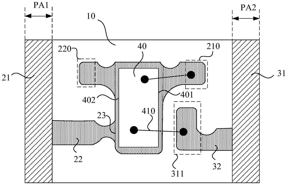
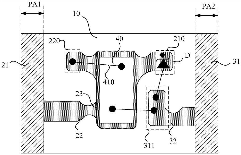
[0031] An embodiment of the present invention provides an LED device, so as to improve the reliability of the LED device and prolong the service life of the device. figure 1 A schematic top view structure diagram of an LED device provided by an embodiment of the present invention, refer to figure 1 , the LED device provided by the embodiment of the present invention includes a bracket and an LED chip 40;

[0032] The bracket includes an insulating substrate 10, a first electrode 20 and a second electrode 30, the ...


PUM


Abstract

The embodiment of the invention discloses an LED device. The LED device comprises a support and an LED chip. The bracket comprises an insulating substrate, and a first electrode and a second electrode which are arranged on the insulating substrate and insulated from each other; the first electrode comprises a first connecting part, a first welding part and a functional part, the root part of the first welding part is connected with the first connecting part, the middle part of the first welding part extends towards the second electrode to form the functional part, the first welding part comprises at least one end part, and the end part of the first welding part is connected with the functional part; the second electrode comprises a second connecting part and a second welding part, and the root of the second welding part is connected with the second connecting part. According to the technical scheme provided by the embodiment of the invention, the proper end part can be selected for wire welding according to the position of the electrode on the LED chip, the extension path of the welding part is designed, and the path of water vapor permeating into the LED device can be prolonged, so that the hydrolysis resistance of the LED device is improved, and the service life of the LED device is prolonged.

Description

technical field [0001] The embodiments of the present invention relate to the technical field of semiconductors, and in particular to an LED device. Background technique [0002] Conventional chip LED devices include brackets, LED chips, bonding wires and encapsulation glue. In the LED device processing process, the LED chip is first fixed on the bracket, and then the two ends of the bonding wire are respectively bonded to the bracket electrode and the LED chip electrode, and finally the LED chip and the bonding wire are covered with encapsulation glue. During the bonding process of the bonding wire, when the distance between the electrode of the LED chip and the edge of the LED chip is relatively long, the bonding wire is likely to touch the edge of the LED chip, resulting in leakage of electricity from the LED device and reducing the reliability of the LED device. During the encapsulation adhesive covering process, due to the difference in material properties between the ...

Claims


Application Information

Patent Timeline
IPC IPC(8): H01L33/62H01L33/48
Inventor 陈燕李军政朱明军邱俊东李友民陈黎敏李红
Owner FOSHAN NATIONSTAR OPTOELECTRONICS CO LTD
Why Eureka
Try Eureka