
Low-voltage noise charge pump circuit

A charge pump, low voltage technology, applied in the direction of conversion equipment without intermediate conversion to AC, can solve the problems of large output ripple, excessive current, voltage, noise, voltage loss, and large current, so as to reduce capacitance loss and reduce noise. , The effect of solving the crosstalk phenomenon

Active Publication Date: 2022-04-12
南京元络芯科技有限公司
View PDF6 Cites 1 Cited by
  • Summary
  • Abstract
  • Description
  • Claims
  • Application Information

AI Technical Summary

Problems solved by technology

The circuit Figure 4 has not done too much noise reduction processing, The original circuit is controlled by two control signals CLK_A and CLK_A_N. When CLK_A_N and CLK_A are switched, there will be simultaneous In the open state, there will be current flowing between each other, resulting in crosstalk, excessive current and voltage noise and output voltage loss, and the current is not limited at the moment the switch is turned on, resulting in The current is very large, so the output ripple and EMI (electromagnetic interference) are large

Method used


Image

  • Low-voltage noise charge pump circuit
  • Low-voltage noise charge pump circuit
  • Low-voltage noise charge pump circuit

Examples


Embodiment 1

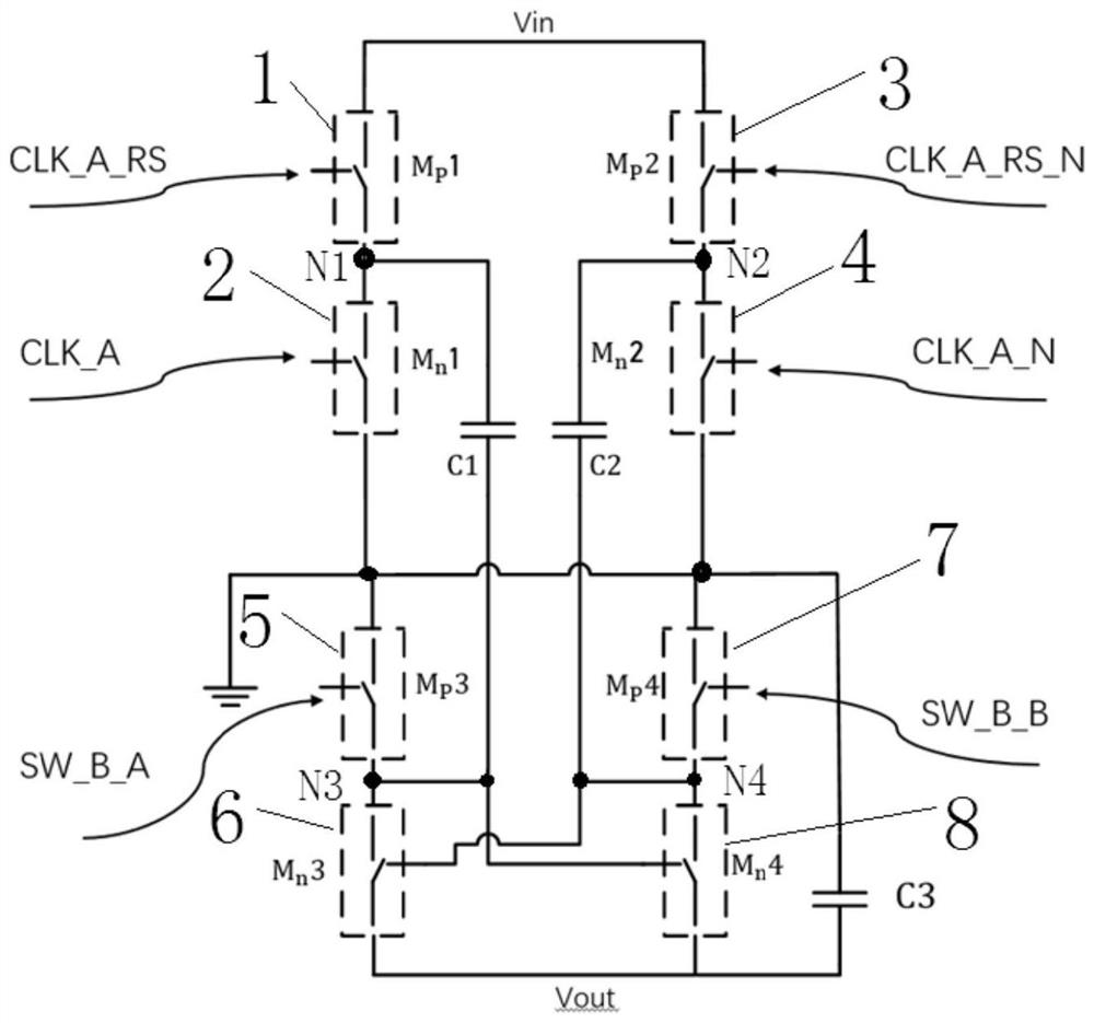
[0031] Example 1: See figure 1 , the low voltage noise charge pump circuit provided in this embodiment includes: a clock unit, a capacitor unit and a switch unit;

[0032] A clock unit, connected to the control terminals of the first controlled switch unit and the second controlled switch unit, for generating non-overlapping clock signals to control switches in the first controlled switch unit and the second controlled switch unit open and close,

[0033] The capacitor unit includes a first pump capacitor C1, a second pump capacitor C2 and a load capacitor C3;

[0034] The switch unit includes a first controlled switch unit connected to the upper plate of the first pump capacitor and the second pump capacitor, and a second controlled switch unit connected to the lower plate of the first pump capacitor and the second pump capacitor, so Both the first controlled switch unit and the second controlled switch unit are controlled by the clock unit signal to enable the input power...

Embodiment 2

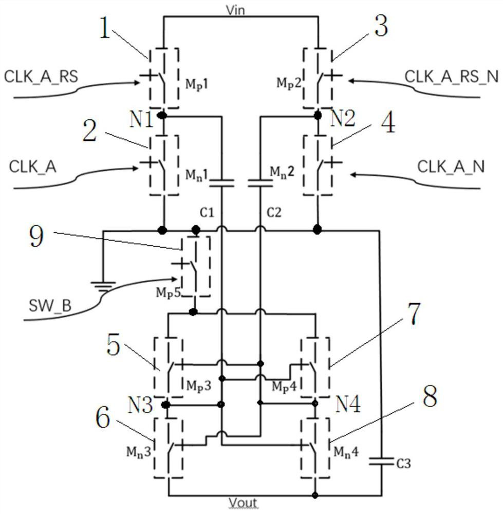
[0051] Embodiment 2: as figure 2 as shown, figure 2 The charge pump circuit shown is in the figure 1 With slight modifications on the basis of , further, the second controlled switch unit also includes a ninth switch 9, such as figure 2 The Mp5 shown, is also the switch for the Mp model. The lower plate of the first pump capacitor C1 is also connected to the seventh switch 7 ( figure 2 Mp4) in the control terminal, the lower plate of the second pump capacitor C2 is also connected to the fifth switch 5 ( figure 2 In Mp3), the first ends of the fifth switch 5 and the seventh switch 7 are connected to the ground GND through the ninth switch, and the control end of the second controlled switch unit is the control end of the ninth switch SW_B.

[0052] figure 2 Among them, Mp1~Mp4 are pmos tubes, Mn1~Mn4 are nmos tubes, they are all used as switches, C1~C3 are capacitors, of which C1, C2 are pump capacitors, C3 is output capacitor, Vin is input voltage, CLK_A_RS, CLK_A...

Embodiment 3

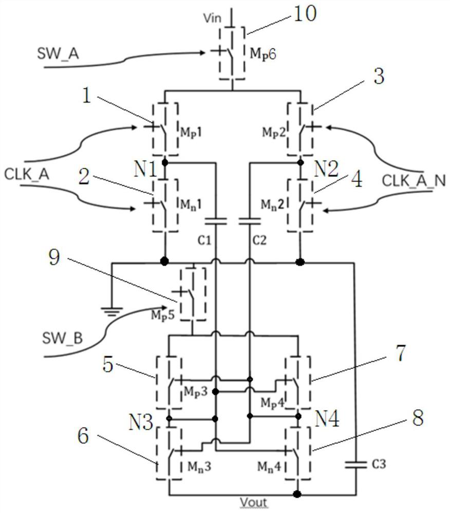
[0054] Embodiment 3: as image 3 As shown, Mp1~Mp4 are pmos tubes, Mn1~Mn4 are nmos tubes, they are all used as switches, C1~C3 are capacitors, among which C1, C2 are pump capacitors, C3 is output capacitor, Vin is input voltage, SW_A , CLK_A_RS, CLK_A, SW_B, CLK_A_RS_N, CLK_A_N are logic control signals.

[0055] image 3 The charge pump circuit shown is in the figure 2 With a slight modification on the basis of the above, the first controlled switch unit further includes a tenth switch 10, the first ends of the first switch 1 and the third switch 3 are connected to the input power supply Vin through the tenth switch 10, the first The control terminals of a controlled switch unit are respectively the control terminals of the first to fourth switches and the control terminal of the tenth switch, wherein the control terminal of the first switch is connected to the control terminal of the second switch, and the control terminal of the third switch The control terminal of the...


PUM


Abstract

The invention discloses a low-voltage noise charge pump circuit. The low-voltage noise charge pump circuit comprises a clock unit, a capacitor unit and a switch unit, the clock unit is used for generating non-overlapping clock signals to control on and off of switches in the first controlled switch unit and the second controlled switch unit, and the capacitor unit comprises a first pump capacitor C1, a second pump capacitor C2 and a load capacitor C3; the switch unit comprises a first controlled switch unit connected to the upper polar plates of the first pump capacitor and the second pump capacitor, and a second controlled switch unit connected to the lower polar plates of the first pump capacitor and the second pump capacitor; the first controlled switch unit and the second controlled switch unit are both controlled by the clock unit signal to be switched on and switched off, so that an input power supply can charge the first pump capacitor and the second pump capacitor, and the first pump capacitor C1 and the second pump capacitor C2 can transfer charged loads to the load capacitor C3. According to the invention, the crosstalk phenomenon between mos transistors can be solved, the noise of the output voltage is reduced, and the circuit efficiency is improved.

Description

technical field [0001] The invention relates to the technical field of semiconductor devices, in particular to a charge pump circuit for reducing output voltage noise. Background technique [0002] With the development of science and technology, semiconductor devices are more and more widely used due to their own characteristics and advantages. Among them, the stability and noise of the charge pump (charge pump) that generates negative pressure in the analog integrated circuit are particularly important. In the actual application process, the noise level of the charge pump output voltage will directly affect the reliability of the circuit where the charge pump is located. [0003] Nowadays, the charge pump uses the charging and discharging of the capacitor to realize the voltage conversion, and the input circuit and the output circuit are turned on in turn. Its internal FET switch array controls the charging and discharging of the flying capacitor in a certain way, so that ...

Claims


Application Information

Patent Timeline
Patent Type & Authority Applications(China)
IPC IPC(8): H02M3/07
CPCY02B70/10
Inventor 张聪潘俊王静波李海涛徐健桂超
Owner 南京元络芯科技有限公司
Learn More