Multi-chip normally-mounted reset wafer level packaging structure and method

A multi-chip, level packaging technology, which is applied in the manufacture of electrical components, electrical solid devices, semiconductor/solid devices, etc., can solve the problems that the chip surface cannot be protected, the chip process is difficult, and the packaging volume is large, so as to reduce the difficulty of cutting , Improving packaging efficiency and simplifying the packaging process

Active Publication Date: 2022-04-15
苏州科阳半导体有限公司
View PDF7 Cites 0 Cited by
  • Summary
  • Abstract
  • Description
  • Claims
  • Application Information

AI Technical Summary

Problems solved by technology

[0003]The above patents have the following disadvantages. First, the anti-overflow components are preset on the packaging substrate, resulting in a large chip pitch and a large overall packaging volume; In the groove of the substrate, the surface of the chip cannot be protected, and the process of placing the chip in the groove is difficult

Method used


Image

  • Multi-chip normally-mounted reset wafer level packaging structure and method
  • Multi-chip normally-mounted reset wafer level packaging structure and method
  • Multi-chip normally-mounted reset wafer level packaging structure and method

Examples


Embodiment Construction

[0037] The following will clearly and completely describe the technical solutions in the embodiments of the present invention with reference to the drawings in the embodiments of the present invention.

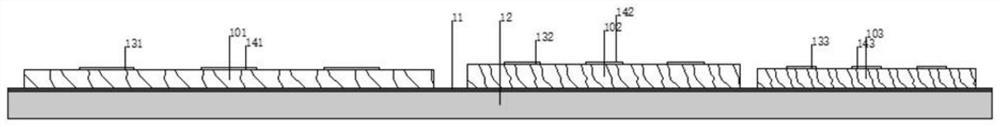
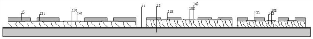
[0038] 1. Multi-chip reset layout, using patch technology to place different types of chips (the number of chips can be flexibly matched, here is an example of 3 chips (101, 102, 103) placed on the substrate 12 with a temporary bonding film 11 , the front of the chip faces up, and the back is attached to the temporary bonding film on the substrate; the front of the chip contains electrodes (each chip includes electrodes 131, 132, 133), key functional areas (such as the IDT area of ​​the surface acoustic filter, the bulk The resonator area of ​​the acoustic wave filter includes key functional areas (141, 142, 143) and other areas in different chips. Taking a group of 3 chips as an example, multiple groups are regularly arranged on the substrate 12 to fill the substrate. shall p...


PUM


Abstract

The invention discloses a multi-chip normally-mounted reset wafer-level packaging structure and method, and the method comprises the following steps: carrying out the reset layout of multiple chips, placing different types of chips 1 on a substrate 12 on which a temporary bonding film 11 is pasted through employing a paster technology, enabling the front surfaces of the chips to be upward, and enabling the back surfaces of the chips to be pasted on the temporary bonding film on the substrate; the front surface of the chip comprises electrodes and key functional areas; manufacturing a first insulating layer, namely manufacturing the first insulating layer 15 on the chip surface of the substrate 12 by utilizing coating, spraying and laminating processes, and performing patterning treatment by utilizing processes such as photoetching and the like to expose part of electrodes and all key functional areas of the chip; and finally, after the rewiring process is completed, the main packaging process is completed, and then the chips are cut into single chips according to the size of each group of chips for subsequent PCB welding. The multi-chip packaging technology belongs to one-time packaging of the multiple chips, the packaging process of the multiple chips is simplified, and the packaging efficiency is improved.

Description

technical field [0001] The invention belongs to the field of semiconductors, and in particular relates to the chip reset and multi-chip packaging technology of filter wafers, and relates to a filter wafer-level packaging structure and method. Background technique [0002] The current packaging process uses flip-chip coating to form a cavity, which has certain requirements for the chip gap. The flip-chip substrate also needs to preset corresponding graphics, and the process is complicated. The patent application number is 201621225249.3, which discloses a thin-film bulk acoustic wave device. The multi-chip module packaging structure including the bare chip includes a substrate and a bare chip. The bare chip includes a thin film bulk acoustic wave device bare chip and other functional bare chips. Corresponding electrodes are provided on the substrate and all the bare chips, and it is characterized in that : All bare chip electrodes are correspondingly connected by gold balls a...

Claims


Application Information

Patent Timeline
Patent Type & Authority Applications(China)
IPC IPC(8): H01L21/56H01L21/78H01L23/31
Inventor 朱其壮陈振国倪飞龙金科吕军
Owner 苏州科阳半导体有限公司
Why Eureka
Try Eureka