
Negative boost circuit in chip and charging and discharging method thereof

A negative boost, charge and discharge technology, applied in electrical components, conversion equipment without intermediate conversion to AC, output power conversion devices, etc., can solve the problem of increased peak current, affecting the normal operation of the image sensor, damage to the circuit system, etc. problem, to achieve the effect of reducing the area, improving the load driving efficiency, and strong driving ability

Pending Publication Date: 2022-04-15
四川创安微电子有限公司
View PDF15 Cites 0 Cited by
  • Summary
  • Abstract
  • Description
  • Claims
  • Application Information

AI Technical Summary

Problems solved by technology

The negative boost circuit realizes charging and discharging through the charge pump. As the required drive capacity of the traditional charge pump circuit increases, the peak current generated by it also increases, and the resulting instantaneous voltage drop will cause damage to the entire circuit system. , and even affect the normal work of the image sensor

Method used


Image

  • Negative boost circuit in chip and charging and discharging method thereof
  • Negative boost circuit in chip and charging and discharging method thereof
  • Negative boost circuit in chip and charging and discharging method thereof

Examples


Embodiment 1

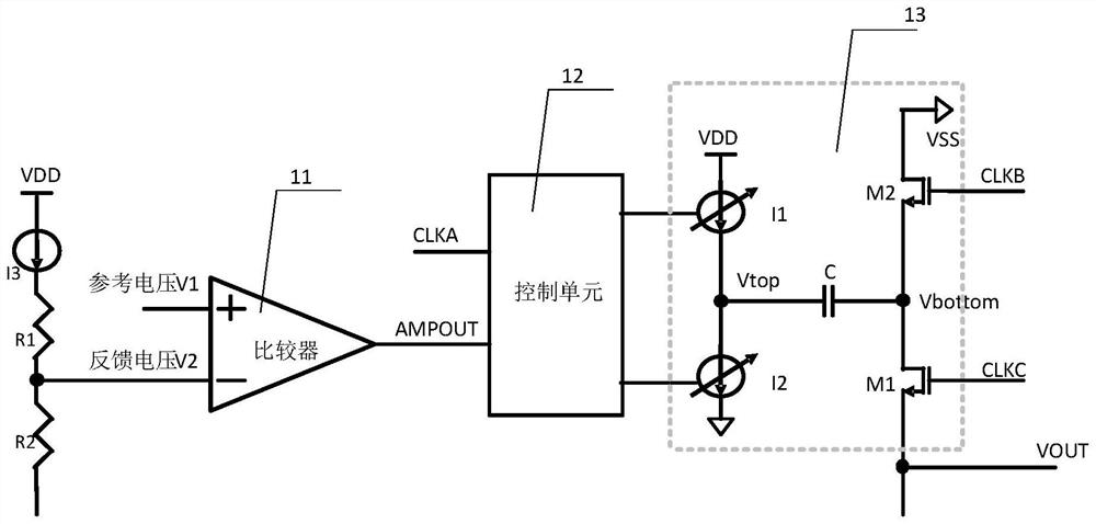
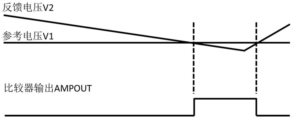
[0036] This embodiment provides an on-chip negative boost circuit, the circuit structure includes a current source I 3 , resistance R 1 , R 2 , comparator 11, control unit 12, charge and discharge unit 13,

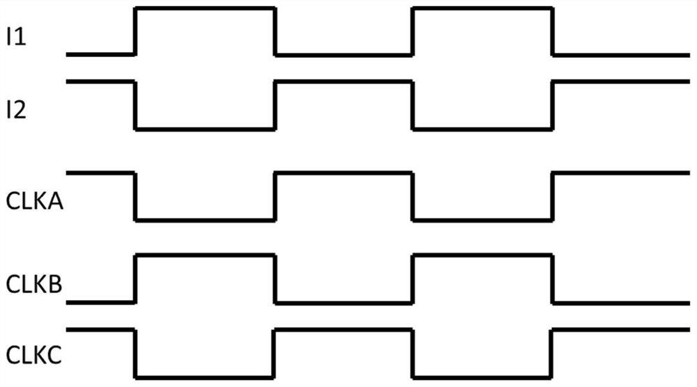
[0037] The charging and discharging unit 13 includes an adjustable current source I 1 , adjustable current source I 2 , capacitor C, N-channel MOS transistors M1 and M2, wherein the adjustable current source I 1 with an adjustable current source I 2 series, adjustable current source I 1 The input terminal is connected to the power supply VDD, and the adjustable current source I 2 The output terminal of the NMOS tube M2 is grounded, the source of M2 is connected to the drain of the NMOS tube M1, the source of M1 is connected to the resistor R2; one end of the capacitor C is connected to the adjustable current source I 1 with an adjustable current source I 2 The common end of the capacitor C, and the other end of the capacitor C is connected to the common end of the ...


PUM


Abstract

The negative boost circuit comprises a current source I3, a resistor R1, a resistor R2, a comparator, a control unit and a charging and discharging unit, the charging and discharging unit comprises an adjustable current source I1, an adjustable current source I2, a capacitor C and N-channel MOS transistors M1 and M2, the adjustable current source I1 and the adjustable current source I2 are connected in series, the input end of the adjustable current source I1 is connected with a power supply VDD, the output end of the adjustable current source I2 is grounded, and the capacitor C is connected with the capacitor C; the drain electrode of the NMOS tube M2 is grounded, the source electrode of the M2 is connected with the drain electrode of the NMOS tube M1, and the source electrode of the M1 is connected with the resistor R2; one end of the capacitor C is connected with the common end of the adjustable current source I1 and the adjustable current source I2, and the other end of the capacitor C is connected with the common end of the source electrode of the M2 and the drain electrode of the M1; and the control unit is used for controlling the current of the adjustable current sources I1 and I2. The invention further provides a negative boost circuit charging and discharging method, peak current can be reduced, the EMI characteristic is good, and the load driving efficiency is effectively improved.

Description

technical field [0001] The invention relates to the technical field of a negative boost circuit, in particular to an in-chip negative boost circuit and a charging and discharging method thereof. Background technique [0002] As image sensors are widely used in mobile phones, notebooks, digital cameras, video game consoles, vehicles, and visual robots, improving imaging quality has become a constant pursuit of image sensor technology, and the pixel size of image sensors is positively related to image quality. Therefore, in order to meet the market demand, the pixel size of the image sensor is getting larger and larger when designing. [0003] When the design size of the pixel continues to increase, various power sources of the image sensor are required to provide greater driving capability. On the other hand, as the frequency range used by wireless devices becomes wider and wider, the anti-electromagnetic interference (EMI) characteristics are also getting more and more atte...

Claims


Application Information

Patent Timeline
IPC IPC(8): H02M3/07H02M1/44
CPCH02M3/07H02M1/44
Inventor 不公告发明人
Owner 四川创安微电子有限公司
Learn More