
High-linearity high-frequency active inductor

An active inductor, high linearity technology, applied in transformer/inductor circuits, etc., can solve the problems of linearity degradation, less than ideal inductor performance, and insufficient coordination

Pending Publication Date: 2022-04-19
BEIJING UNIV OF TECH
View PDF0 Cites 0 Cited by
  • Summary
  • Abstract
  • Description
  • Claims
  • Application Information

AI Technical Summary

Problems solved by technology

[0004] At present, the existing active inductance circuit, due to the relatively simple circuit structure, the components are not optimized enough, the coordination is not enough, the inductance performance is not ideal, especially the lack of excellent comprehensive performance, especially at high frequencies
On the one hand, active inductors still have problems such as small inductance and low Q value at high frequencies
On the other hand, active inductors also face the problem of low linearity, that is, when the amplitude of the input signal or bias current changes greatly, the transconductance value of the transistor will change greatly, which will cause the inductance circuit to be equal. Large changes in the effective inductance value and Q value cause linearity degradation
The low linearity of the inductor will deteriorate the performance of the integrated circuit, such as increasing the phase noise of the VCO, etc.
These problems greatly limit the application of active inductors in integrated circuits

Method used


Image

  • High-linearity high-frequency active inductor
  • High-linearity high-frequency active inductor
  • High-linearity high-frequency active inductor

Examples


Embodiment Construction

[0022] In order to make the object, technical solution and advantages of the present invention clearer, the present invention will be further described below in conjunction with the accompanying drawings.

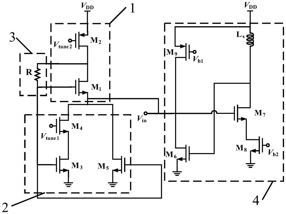
[0023] figure 1 is an embodiment of the active inductance circuit. It includes: an adjustable positive transconductance unit (1), an adjustable linear negative transconductance unit (2), a feedback unit (3), and an equivalent negative capacitance-negative resistance unit (4).

[0024] In the embodiment of the active inductance circuit, the adjustable positive transconductance unit (1) in the high linearity active inductance circuit comprises a first N-type MOS transistor (M 1 ), the second P-type MOS transistor (M 2 ); the adjustable high linear negative transconductance unit (2) includes the third N-type MOS transistor (M 3 ), the fourth N-type MOS transistor (M 4 ), the fifth N-type MOS transistor (M 5 ); the feedback unit (3) includes a feedback resistor (R); the eq...


PUM


Abstract

The invention discloses a high-linearity high-frequency active inductor, and belongs to the field of circuits. The high-linearity high-frequency active inductor comprises an adjustable positive transconductance unit (1), an adjustable high-linearity negative transconductance unit (2), a feedback unit (3) and an equivalent negative capacitance-negative resistance unit (4). The output end of the adjustable positive transconductance unit (1) is connected with the first end of the feedback unit (3), the second end of the feedback unit (3) is connected with the input end of the adjustable high-linearity negative transconductance unit (2), and the output end of the adjustable high-linearity negative transconductance unit (2) is simultaneously connected with the input end of the adjustable positive transconductance unit (1) and is connected with the equivalent negative capacitance-negative resistance unit (4) in parallel. Through the division and cooperation of the four units and the two adjusting ends (Vtune1 and Vtune2) of the four units, the grid electrode of a first N-type MOS transistor (M1) in the adjustable transconductance unit (1) achieves self-bias, and the active inductor has the comprehensive performance of being wide in frequency band, large in inductance value and Q value under high frequency, adjustable, high in linearity and the like.

Description

technical field [0001] The invention relates to the design fields of radio frequency devices and integrated circuits, in particular to an active inductance circuit with large inductance value and Q value, adjustability and high linearity under wide frequency band and high frequency. Background technique [0002] With the rapid development of microelectronics technology, the size of transistor active devices in integrated circuits continues to shrink and their performance continues to improve, while the performance of on-chip passive devices is improving slowly, and their performance is closely related to geometric dimensions, which hinders the development of integrated circuits. The size of the device shrinks and the performance improves proportionally with the shrinking of the size of the active device. Therefore, a solution is urgently needed for on-chip passive devices. [0003] Passive spiral inductors, one of the commonly used on-chip passive devices in integrated circ...

Claims


Application Information

Patent Timeline
IPC IPC(8): H01F27/42
CPCH01F27/42
Inventor 张万荣王晓雪张思佳谢红云金冬月那伟聪李白
Owner BEIJING UNIV OF TECH
Learn More