All-enclosed gate device and manufacturing method thereof
A technology of fully enclosing gates and manufacturing methods, which is applied in semiconductor/solid-state device manufacturing, semiconductor devices, electrical components, etc., can solve the problems of power consumption and manufacturing cost reduction, and the computing power of field effect transistor devices needs to be improved, so as to reduce the production cost. Effects of cost, low power consumption, and high operating performance
- Summary
- Abstract
- Description
- Claims
- Application Information
AI Technical Summary
Problems solved by technology
Method used
Image
Examples
Embodiment 1
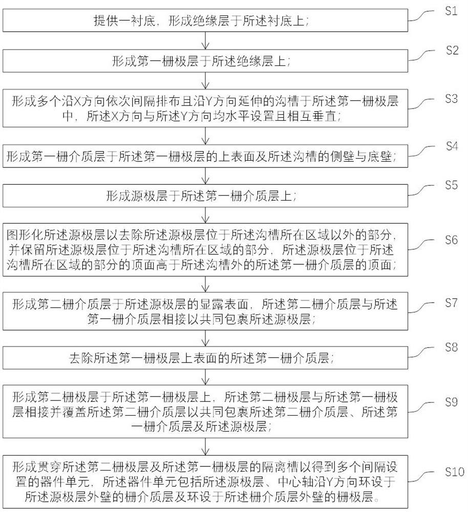
[0061] The present embodiment provides a method for fabricating a gate-all-around device. Please refer to FIG. 1, which shows a process flow of the method.
[0063] S2: forming a first gate layer on the insulating layer;
[0064] S3: forming a plurality of trenches that are sequentially spaced along the X direction and extend along the Y direction in the first gate layer,
[0065] S4: forming a first gate dielectric layer on the upper surface of the first gate layer and the sidewalls and bottom walls of the trench;
[0066] S5: forming a source layer on the first gate dielectric layer;
[0067] S6: patterning the source layer to remove a portion of the source layer outside the area where the trench is located, and
[0068] S7: forming a second gate dielectric layer on the exposed surface of the source layer, the second gate dielectric layer and the first gate dielectric layer
[0069] S8: remove the first gate dielectric layer on the upper surface of the first gate layer;
[0070] ...
Embodiment 2
[0108] This embodiment adopts basically the same technical solution as the first embodiment, the difference is that the source layer is removed
[0109] Please refer to FIG. 26, which shows a process flow diagram of the manufacturing method of the gate-all-around device of the present embodiment, including the following steps:
[0110] S1: a substrate is provided, and an insulating layer is formed on the substrate;
[0111] S2: forming a first gate layer on the insulating layer;
[0112] S3: forming a plurality of trenches that are sequentially spaced along the X direction and extend along the Y direction in the first gate layer,
[0113] S4: forming a first gate dielectric layer on the upper surface of the first gate layer and the sidewalls and bottom walls of the trench;
[0114] S5: forming a source layer on the first gate dielectric layer;
[0115] S6: thin the source layer until the top surface of the source layer is not higher than the first gate dielectric outside the trench...
PUM
| Property | Measurement | Unit |
|---|---|---|
| thickness | aaaaa | aaaaa |
| thickness | aaaaa | aaaaa |
Abstract
Description
Claims
Application Information


