Shielding film for wireless charging and preparation method and manufacturing equipment thereof
A technology for wireless charging and manufacturing equipment, applied in electrical components, circuit devices, vacuum evaporation coating, etc., can solve the problems of low saturation magnetic induction intensity, low electromagnetic induction coupling efficiency, maximum output power, and small upper limit of charging speed, etc. The effect of high saturation magnetic induction intensity and resonance frequency, improving wireless charging power, and improving magnetic coupling efficiency
- Summary
- Abstract
- Description
- Claims
- Application Information
AI Technical Summary
Problems solved by technology
Method used
Image
Examples
preparation example Construction
[0034] A method for preparing a shielding film for wireless charging, comprising the following steps,
[0035] Obtain single-sided adhesive, which includes sequentially stacked release film, adhesive layer and protective film;
[0036] Tear film, tear off the protective film of the single-sided adhesive tape;
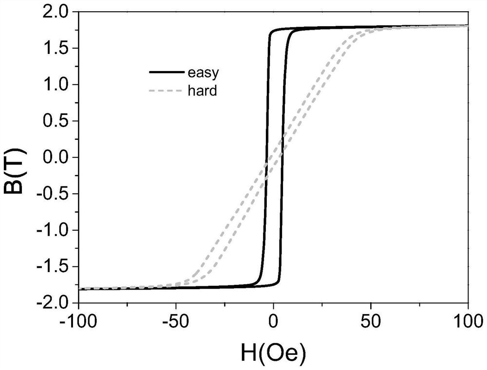
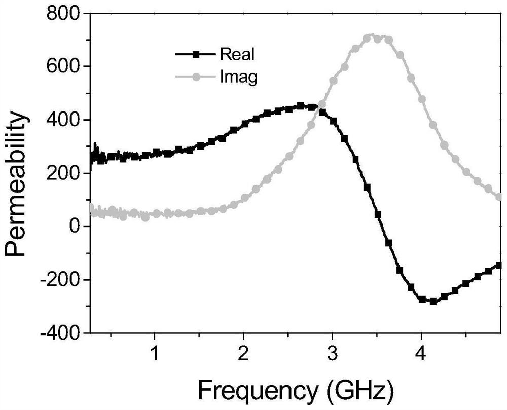
[0037] Magnetron sputtering, performing magnetron sputtering on the surface of the glue layer away from the release film to form a magnetic layer on the surface of the glue layer away from the release film to obtain a shield for wireless charging film, the magnetic layer is (Fe 65 co 35 ) x (TiO 2 ) 1-x layer, wherein, x≥0.76; the saturation magnetic induction B of the magnetic layer s ≥1.7T.
[0038] As can be seen from the above description, the beneficial effect of the present invention is that the method for preparing the shielding film for wireless charging adopts magnetron sputtering and only needs one step to deposit the magnetic thin film material on the ...
Embodiment 1
[0049] Please refer to Figure 1 to Figure 5 , Embodiment 1 of the present invention is: a shielding film for wireless charging, which is applied to the receiving end of wireless charging, and is especially suitable for high-frequency working conditions.
[0050] Such as figure 1 As shown, the shielding film for wireless charging includes an adhesive layer 1 and a magnetic layer 2 formed on one surface of the adhesive layer 1 by magnetron sputtering, and the other surface of the adhesive layer 1 opposite to the magnetic layer 2 A release film 3 is provided, that is to say, among the two opposite surfaces of the adhesive layer 1 , the magnetic layer 2 is deposited on one surface, and the release film 3 is provided on the other surface. During use, the user can fix the magnetic layer 2 on the external member through the adhesive layer 1 by tearing off the release film 3 .
[0051] The magnetic layer 2 is (Fe 65 co 35 ) x (TiO 2 ) 1-x layer, wherein, x≥0.76; the saturation...
Embodiment 2
[0054] Please refer to Figure 6 , Embodiment 2 of the present invention is a preparation method for preparing the wireless charging shielding film described in Embodiment 1, comprising the following steps,
[0055] A single-sided adhesive is obtained, and the single-sided adhesive includes a release film, an adhesive layer, and a protective film stacked in sequence; in this embodiment, the width of the single-sided adhesive is 50 mm, and the thickness is 80 μm.
[0056] Tear film, tear off the protective film of the single-sided adhesive tape;
[0057] Magnetron sputtering, performing magnetron sputtering on the surface of the glue layer away from the release film to form a magnetic layer on the surface of the glue layer away from the release film to obtain a shield for wireless charging film, the magnetic layer is (Fe 65 co 35 ) x (TiO 2 ) 1-x layer, wherein, x≥0.76; the saturation magnetic induction B of the magnetic layer s ≥1.7T. It is easy to understand that in o...
PUM
| Property | Measurement | Unit |
|---|---|---|
| Resonant frequency | aaaaa | aaaaa |
| width | aaaaa | aaaaa |
| thickness | aaaaa | aaaaa |
Abstract
Description
Claims
Application Information


