High density electrical connectors

A connector and high-level technology, applied in the direction of electrical connection formation of printed components, electrical solid devices, circuits, etc., can solve the problems of increased danger, increased difficulty, high-precision active alignment and accelerated cost, and achieve easy repair and easy replacement Effect

Inactive Publication Date: 2004-04-07
INFINEON TECH AG
View PDF1 Cites 0 Cited by
  • Summary
  • Abstract
  • Description
  • Claims
  • Application Information

AI Technical Summary

Problems solved by technology

As density increases, alignment requirements increase, and the higher this requirement becomes, the more important it is to use self-alignment because of the increased cost of high-precision active alignment acceleration
[0007] When connecting different parts of a complex system, as the complexity of the system increases, so does the danger of having to replace some or more of these parts in order to obtain an efficient system
Increased difficulty in adequately testing components at relevant frequencies and operating conditions

Method used


Image

  • High density electrical connectors
  • High density electrical connectors
  • High density electrical connectors

Examples


Embodiment Construction

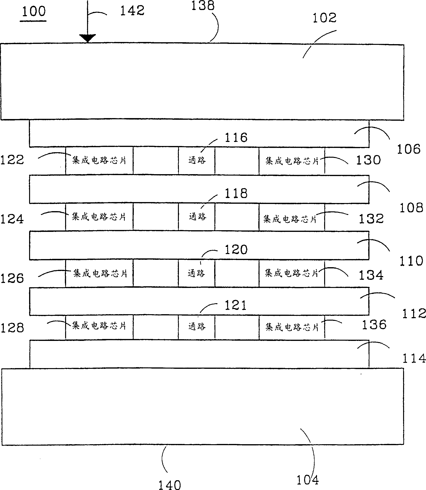
[0028] The invention can be used in a variety of microelectronic systems for the alignment of resilient electrical contacts and internally mounted chips. The invention can be used in multi-chip modules, especially where it is difficult to determine the quality of the chips before mounting them. The present invention can be used where there are many problems today, for example, where there are flip-chips, or where there is a large mismatch in the coefficient of thermal expansion between the board and the chip. Repairs can often be dangerous and expensive, and, in some types of MCM devices, are essentially impossible.

[0029] figure 1 An example is shown where the invention can be used, but the invention is not limited to this field. The invention can of course be used in any kind of microsystem, even submicrosystems. figure 1 A cross-section of a three-dimensional (3D) multi-chip module 100 is shown. The three-dimensional module consists of two-dimensional (2D) multi-chip ...


PUM


Abstract

The present invention relates to self-aligned, flexible high density and impedance adjusted electrical connectors used in microelectronic systems. This invention solves the problem of having electrical connection and alignment at the same time. One connector (200) having a first part (204) consists of two metal layer structures, a first signal path (212) and a first ground path (210), covering the V-groove (202). The connector also has a second part (208) consisting of corresponding metal layers, a second signal path (224) covering the elastic bump (206) and a second signal ground plane (226), which fits into the V-groove (202). The first and the second signal path (212, 224) are in contact with each other when the first and the second part (204, 208) are brought together. The contact is self-aligned when put together. The electrical contact will remain even if displaced due to the thermal expansion.

Description

technical field [0001] This invention relates to the interconnection of electrical devices and, more particularly, to self-aligning deformable high density electrical connectors with adjustable impedance. Background technique [0002] Technological developments in the field of integrated circuits (ICs) have created a demand for faster and more compact systems. Lightweight and compact construction is a requirement in itself in many applications. Technological development also tends towards more complex systems, which include more and more components that need to be connected to each other. In order for the new system to meet the requirements for fast access between the different components, the length of the paths between the different components of the system must be kept within certain limits. [0003] As the complexity of the system increases, the length of the paths between components also increases. In order not to exceed the maximum usable distance between these part...

Claims


Application Information

Patent Timeline
Patent Type & Authority Patents(China)
IPC IPC(8): H01L21/60H01L21/98H01L23/498H01L23/538H01L23/66H01L27/00H01L29/06H05K3/32H05K3/40
CPCH01L2224/81141H01L2224/81801H01L23/66H01L23/5383H05K3/326H01L2924/01006H01L2924/3025H01L23/49811H01L2924/3011H01L2924/01079H01L2924/14H01L2224/81365H01L2224/16237H01L29/0657H01L2924/01005H01L2924/01024H01L2924/01082H01L25/50H01L2924/30107H01L2924/014H01L2924/01023H05K3/4007H01L2924/30105H01L23/49822H01L2224/81136H01L2924/01077H01L2924/01033H01L2224/16147H01L24/81H01L2924/0102H01L2924/01075H01L29/41
Inventor L·H·赫瑟尔波姆J·P·博德
Owner INFINEON TECH AG
Why Eureka
Try Eureka