MOSFET (Metal-Oxide-Semiconductor Field Effect Transistor) device integrated with PiN structure temperature sensor and preparation method of MOSFET device

A temperature sensor and device technology, applied in the field of microelectronics, can solve the problems affecting the application reliability of the device, the characteristics are deteriorated, and the thermal characteristics of the device cannot be accurately obtained, and the effect of improving the thermal reliability is achieved.

Pending Publication Date: 2022-05-24
瑶芯微电子科技(上海)有限公司
View PDF3 Cites 0 Cited by
  • Summary
  • Abstract
  • Description
  • Claims
  • Application Information

AI Technical Summary

Problems solved by technology

[0004] However, in conventional 4H-SiC power MOSFET devices with traditional structures, there is no such internal monitoring device, and the internal thermal characteristics of the device cannot be accurately obtained by using external devices
This will lead to the deterioration of the characteristics of the device when it works at high temperature, thus affecting the application reliability of the device

Method used


Image

  • MOSFET (Metal-Oxide-Semiconductor Field Effect Transistor) device integrated with PiN structure temperature sensor and preparation method of MOSFET device
  • MOSFET (Metal-Oxide-Semiconductor Field Effect Transistor) device integrated with PiN structure temperature sensor and preparation method of MOSFET device
  • MOSFET (Metal-Oxide-Semiconductor Field Effect Transistor) device integrated with PiN structure temperature sensor and preparation method of MOSFET device

Examples


Embodiment 1

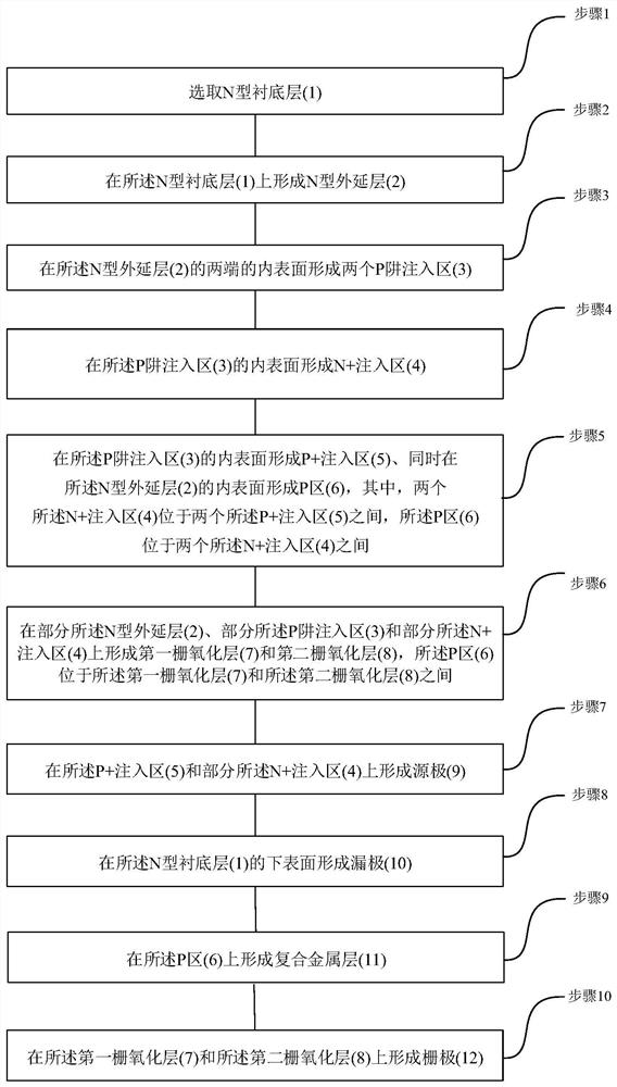
[0051] See figure 1 , Figures 2a-2j , figure 1 A flow chart of a method for manufacturing a MOSFET device with an integrated PiN structure temperature sensor provided by an embodiment of the present invention, Figures 2a-2j A process schematic diagram of a MOSFET device integrating a PiN structure temperature sensor provided by an embodiment of the present invention. The invention provides a method for preparing a MOSFET device with an integrated PiN structure temperature sensor, the preparation method comprising the following steps:

[0052] Step 1, see Figure 2a , select the N-type substrate layer 1 .

[0053] Specifically, the N-type substrate layer 1 is selected, and the N-type substrate layer 1 is cleaned using an RCA cleaning standard.

[0054] Further, the N-type substrate layer 1 is an N-type 4H-SiC substrate layer.

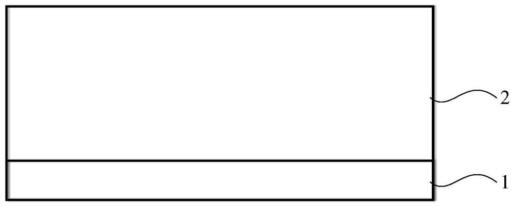
[0055] Step 2, see Figure 2b , forming an N-type epitaxial layer 2 on the N-type substrate layer 1 .

[0056] Specifically, an N-type epitaxi...

Embodiment 2

[0098] See image 3 , image 3 A schematic structural diagram of a MOSFET device integrating a PiN structure temperature sensor provided by an embodiment of the present invention. The present invention proposes a MOSFET device integrating a PiN structure temperature sensor. The MOSFET device is prepared by the preparation method described in Embodiment 1. The MOSFET device includes:

[0099] N-type substrate layer 1;

[0100] The N-type epitaxial layer 2 is located on the N-type substrate layer 1;

[0101] Two P-well injection regions 3 are respectively located at both ends of the N-type epitaxial layer 2;

[0102] Two N+ implantation regions 4 are respectively located in the two P well implantation regions 3;

[0103] Two P+ implant regions 5 are respectively located in the two P well implant regions 3, and the two N+ implant regions 4 are located between the two P+ implant regions 5;

[0104] The P region 6 is located in the N-type epitaxial layer 2, and the P region 6 ...


PUM

PropertyMeasurementUnit
thicknessaaaaaaaaaa

Abstract

The invention relates to an MOSFET (Metal-Oxide-Semiconductor Field Effect Transistor) device integrated with a PiN structure temperature sensor and a preparation method of the MOSFET device. The method comprises the following steps: selecting an N-type substrate layer; forming an N-type epitaxial layer on the N-type substrate layer; forming P well injection regions on the inner surfaces of the two ends of the N-type epitaxial layer; forming an N + injection region on the inner surface of the P well injection region; forming a P + injection region on the inner surface of the P well injection region, and forming a P region on the inner surface of the N-type epitaxial layer; forming a first gate oxide layer and a second gate oxide layer on a part of the N-type epitaxial layer, a part of the P well injection region and a part of the N + injection region; forming a source electrode on the P + injection region and a part of the N + injection region; forming a drain electrode on the lower surface of the N-type substrate layer; forming a composite metal layer on the P region; and forming a gate on the first gate oxide layer and the second gate oxide layer. The temperature sensor with the PiN structure can monitor thermal characteristics such as thermal distribution and junction temperature in an MOSFET device body in real time by testing the change of current, so as to guide the change of the working state of the device.

Description

technical field [0001] The invention belongs to the technical field of microelectronics, and relates to a MOSFET device integrating a PiN structure temperature sensor and a preparation method thereof. Background technique [0002] Silicon carbide (SiC) has become one of the most advantageous semiconductor materials for manufacturing high-temperature, high-power electronic devices due to its excellent physical, chemical and electrical properties, and has a power device quality factor much greater than that of Si materials. The research and development of SiCMOSFET (Metal-Oxide-Semiconductor Field-Effect Transistor, Metal-Oxide-Semiconductor Field-Effect Transistor) power devices began in the 1990s. It has a series of advantages such as high input impedance, fast switching speed, high operating frequency, and high temperature and high pressure resistance. , has been widely used in switching regulated power supply, high-frequency heating, automotive electronics and power amplif...

Claims


Application Information

Patent Timeline
Patent Type & Authority Applications(China)
IPC IPC(8): H01L21/336H01L23/34H01L29/78
CPCH01L29/7803H01L29/7831H01L29/7815H01L23/34H01L29/66068
Inventor 李鑫
Owner 瑶芯微电子科技(上海)有限公司
Why Eureka
Try Eureka