Semiconductor device and forming method
A semiconductor and device technology, applied in the field of semiconductor devices and formation, can solve the problems of high material cost, wafer processing cost, material loss, etc., and achieve the effect of reducing the risk of fragmentation, reducing material cost, and not easy to break
- Summary
- Abstract
- Description
- Claims
- Application Information
AI Technical Summary
Problems solved by technology
Method used
Image

Examples
Embodiment Construction
[0027] The technical solutions in the embodiments of the present application will be clearly and completely described below with reference to the accompanying drawings. Obviously, the described embodiments are only a part of the embodiments of the present application, but not all of the embodiments. Based on the embodiments in this application, all other embodiments obtained by those skilled in the art without creative efforts shall fall within the protection scope of this application. In the case of no conflict, the following various embodiments and their technical features can be combined with each other.
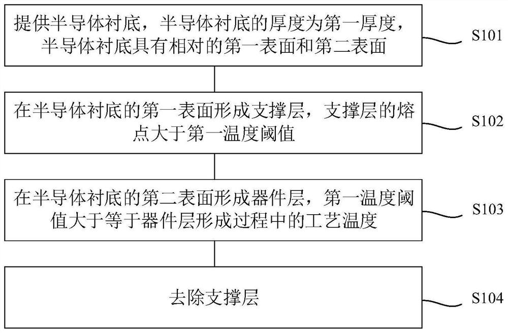
[0028] Please refer to figure 1 , which is a schematic flowchart of a method for forming a semiconductor device according to an embodiment of the present application.
[0029] The method for forming a semiconductor device in this embodiment includes the following steps:
[0030] Step S101 , providing a semiconductor substrate, the thickness of the semiconductor substrat...
PUM
| Property | Measurement | Unit |
|---|---|---|
| thickness | aaaaa | aaaaa |
| thickness | aaaaa | aaaaa |
| thickness | aaaaa | aaaaa |
Abstract
Description
Claims
Application Information
 - R&D
- Intellectual Property
- Life Sciences
- Materials
- Tech Scout
- Unparalleled Data Quality
- Higher Quality Content
- 60% Fewer Hallucinations
Browse by: Latest US Patents, China's latest patents, Technical Efficacy Thesaurus, Application Domain, Technology Topic, Popular Technical Reports.
© 2025 PatSnap. All rights reserved.Legal|Privacy policy|Modern Slavery Act Transparency Statement|Sitemap|About US| Contact US: help@patsnap.com