Semiconductor packaging structure and manufacturing method thereof

A technology of packaging structure and manufacturing method, applied in semiconductor/solid-state device manufacturing, semiconductor devices, semiconductor/solid-state device components, etc., can solve problems such as limited application fields, decreased accuracy, environmental pollution, etc., to increase electrical performance, The effect of reducing package height and improving accuracy

Pending Publication Date: 2022-05-27
PHOENIX PIONEER TECH
View PDF0 Cites 1 Cited by
  • Summary
  • Abstract
  • Description
  • Claims
  • Application Information

AI Technical Summary

Problems solved by technology

[0007] (1) The package structure uses lead frames and bridging copper sheets, so the height (thickness) of the package cannot be reduced, which limits its application field
[0008] (2) Solder or solder paste contains a relatively high proportion of lead, and lead metal will cause environmental pollution and have a considerable impact on human health
[0009] (3) Each component may be displaced before the high-temperature reflow process at 380 degrees Celsius fixes all components, resulting in a decrease in accuracy

Method used


Image

  • Semiconductor packaging structure and manufacturing method thereof
  • Semiconductor packaging structure and manufacturing method thereof
  • Semiconductor packaging structure and manufacturing method thereof

Examples


Embodiment Construction

[0053] The technical solutions in the embodiments of the present invention will be clearly and completely described below with reference to the accompanying drawings in the embodiments of the present invention. In the following description, many specific details are set forth to facilitate a full understanding of the present invention, but the present invention can also be implemented in other ways different from those described herein, and those skilled in the art can do so without departing from the connotation of the present invention. Similar promotion, therefore, the present invention is not limited by the specific embodiments disclosed below.

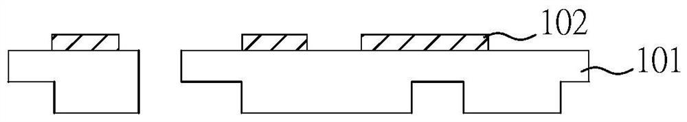
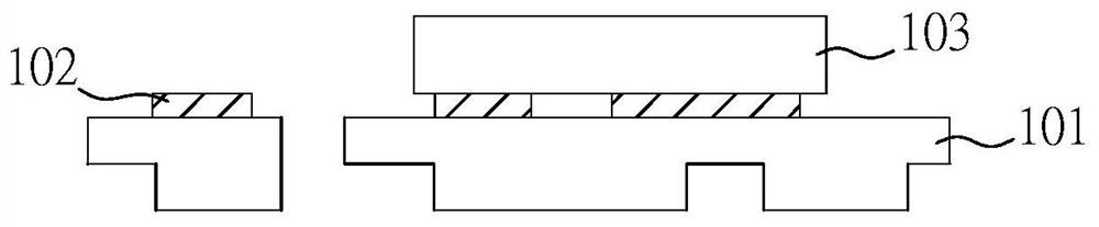
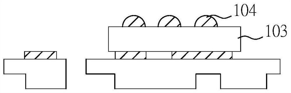
[0054] Please refer to figure 2 As shown, the first state embodiment of the semiconductor package structure 2 of the preferred embodiment of the present invention includes a first stack structure 20 and a second stack structure 30 . The second stack structure 30 is stacked on the first stack structure 20 . The first stacked str...


PUM


Abstract

The invention provides a semiconductor packaging structure and a manufacturing method thereof. The semiconductor packaging structure comprises a first stacking structure and a second stacking structure which are stacked, the first stacked structure comprises a first dielectric layer, a first power chip, a first conductive connecting element, a first conductive column and a first patterned conductive layer; the second stacked structure comprises a second dielectric layer, a second power chip, a second conductive connecting element, a second conductive column, a second patterned conductive layer and a third patterned conductive layer; a first power wafer and a second power wafer are stacked up and down so as to provide a semiconductor packaging structure in which the first power wafer and the second power wafer can be directly and electrically connected through a circuit structure and related defects of a lead frame can be eliminated. In addition, the invention also provides a manufacturing method of the semiconductor packaging structure.

Description

technical field [0001] The present invention relates to a package structure and a manufacturing method thereof, in particular to a semiconductor package structure and a manufacturing method thereof. Background technique [0002] With the substantial increase in the demand for information and automotive electronics, the package structure of the Quad Flat No-Lead (QFN) package has been widely used because of its better heat dissipation effect, lower impedance value and anti-electromagnetic interference. Become an important semiconductor packaging technology. [0003] In the QFN structure, the copper clip technology is a technology developed to meet high power requirements. The copper sheet is designed in the shape of an arch bridge with a high and low drop. The copper sheet is bonded to the chip by a solder dispenser. It has a small impedance to carry a large current and can withstand deformation caused by thermal stress, so it is suitable for Such as high power components s...

Claims


Application Information

Patent Timeline
Patent Type & Authority Applications(China)
IPC IPC(8): H01L23/522H01L23/528H01L25/07H01L21/768
CPCH01L23/528H01L23/5226H01L25/071H01L25/50H01L21/6835H01L23/5389H01L2224/18H01L2224/32245H01L2224/40245H01L2224/82H01L2221/68345H01L2224/73267H01L24/92H01L24/24H01L24/73H01L25/16H01L2224/92244H01L2224/24137H01L2224/24146H01L2924/13091H01L24/82H01L2224/82005H01L2224/82101H01L2224/82106
Inventor 许哲玮
Owner PHOENIX PIONEER TECH
Why Eureka
Try Eureka