

LED epitaxial structure and preparation method thereof
A technology of epitaxial structure and confinement layer, applied in the direction of final product manufacturing, sustainable manufacturing/processing, climate sustainability, etc., can solve the problem of high difficulty of epitaxial preparation process, reduce growth warpage, avoid preparation process, reduce process The effect of preparation difficulty and cost
Pending Publication Date: 2022-05-27
XIAMEN SILAN ADVANCED COMPOUND SEMICON CO LTD
View PDF0 Cites 0 Cited by
- Summary
- Abstract
- Description
- Claims
- Application Information
AI Technical Summary
Problems solved by technology
However, the p-type semiconductor layer in the semiconductor device includes a p-type DBR layer located between the tunneling layer and the p-type confinement layer, and the epitaxial preparation process of the p-type DBR layer is relatively difficult
Method used
View moreImage
Smart ImageViewing Examples

Examples
preparation example Construction
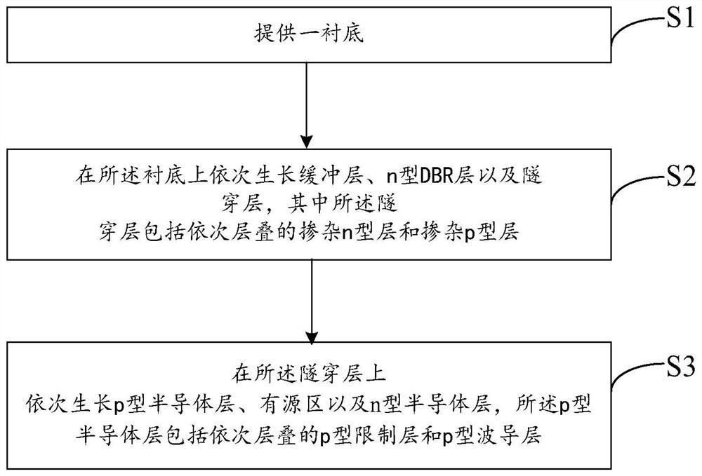
[0048] see figure 2 , the preparation method of the LED epitaxial structure 20 specifically includes the following steps:
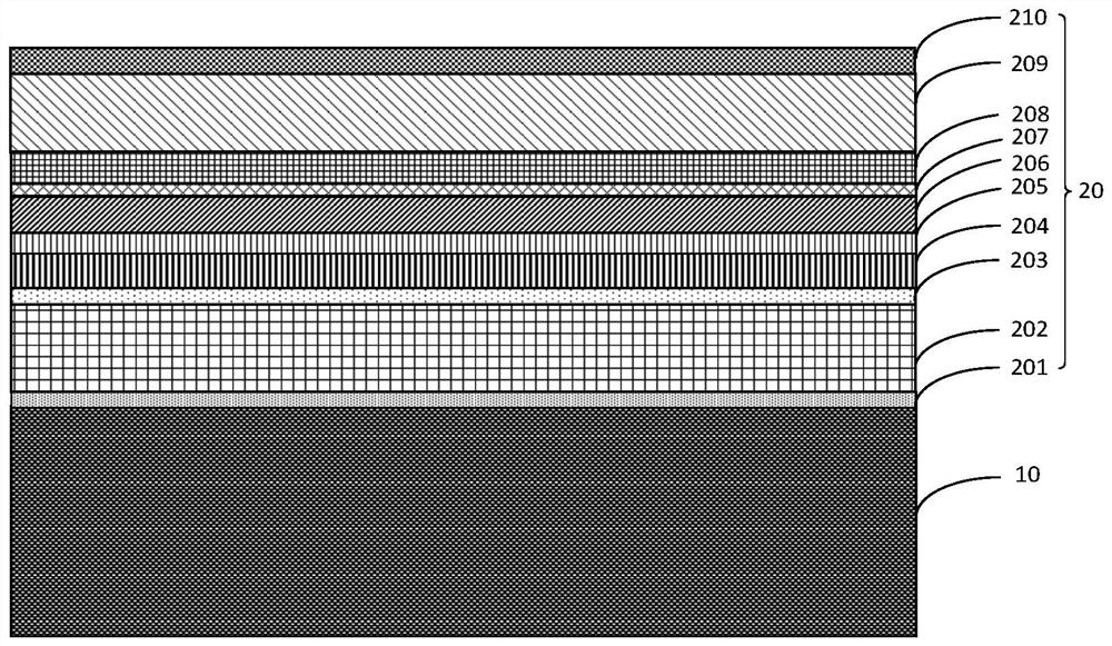
[0049] Step S1: providing a substrate 10;
[0050] Step S2 : growing a buffer layer 201 , an n-type DBR layer 202 and a tunneling layer 203 sequentially on the substrate 10 , wherein the tunneling layer 203 includes a doped n-type layer and a doped p-type layer stacked in sequence.
[0051] Step S3 : growing a p-type semiconductor layer, an active layer 206 and an n-type semiconductor layer in sequence on the tunneling layer 203 , where the p-type semiconductor layer includes a p-type confinement layer 204 and a p-type waveguide layer 205 stacked in sequence.
Login to View More PUM
| Property | Measurement | Unit |
|---|---|---|
| thickness | aaaaa | aaaaa |
| wavelength | aaaaa | aaaaa |
| thickness | aaaaa | aaaaa |
Abstract
The invention provides an LED epitaxial structure and a preparation method thereof.The LED epitaxial structure sequentially comprises a buffer layer, an n-type DBR layer, a tunneling layer, a p-type semiconductor layer, an active layer and an n-type semiconductor layer from bottom to top, the buffer layer, the n-type DBR layer, the tunneling layer, the p-type semiconductor layer, the active layer and the n-type semiconductor layer are located on a substrate, and the p-type semiconductor layer comprises a p-type limiting layer and a p-type waveguide layer which are sequentially stacked; the tunneling layer comprises a doped n-type layer and a doped p-type layer which are stacked in sequence. According to the epitaxial structure, the tunneling layer is introduced between the n-type DBR layer and the p-type limiting layer, so that stress generated by lattice mismatch between the n-type DBR layer and the p-type limiting layer can be reduced, and growth warping of the epitaxial structure can be reduced; and the tunneling layer can also provide tunneling current, so that a reverse PN junction formed by the n-type DBR layer and the p-type limiting layer is conducted. In addition, the preparation method of the LED epitaxial structure is simple.
Description
technical field [0001] The invention relates to the technical field of semiconductors, in particular to an LED epitaxial structure and a preparation method thereof. Background technique [0002] Light Emitting Diode (LED) is an electronic component that directly converts electrical energy into light energy by generating photons through the radiative recombination of conduction band electrons and valence band holes in semiconductor materials. LEDs have been widely used in many high-efficiency solid-state lighting fields. The traditional red LED epitaxial structure is "p-side up", that is, an n-type semiconductor layer, an active layer, and a p-type semiconductor layer are sequentially grown on an n-type GaAs substrate. For red LED chips, the GaAs substrate will strongly absorb the red light emitted by the active layer, resulting in low luminous efficiency of the red LED. In order to improve the luminous efficiency of LED, on the basis of the original structure, a DBR struct...
Claims
Login to View More Application Information
Patent Timeline
 Patent Type & AuthorityApplications(China)
IPC IPC(8): H01L33/12H01L33/10H01L33/14H01L33/00
CPCH01L33/10H01L33/12H01L33/14H01L33/0062Y02P70/50
Inventor王亚宏李森林杨美佳毕京锋
OwnerXIAMEN SILAN ADVANCED COMPOUND SEMICON CO LTD