
Packaging module, preparation method thereof, base station and electronic equipment

A molding and substrate technology, applied in the direction of circuits, electrical components, electrical solid devices, etc., can solve the problems of increasing the occupied area of ​​the packaging structure 1, signal signal crosstalk, cavity height, etc.

Pending Publication Date: 2022-05-31
HUAWEI TECH CO LTD
View PDF0 Cites 1 Cited by
  • Summary
  • Abstract
  • Description
  • Claims
  • Application Information

AI Technical Summary

Problems solved by technology

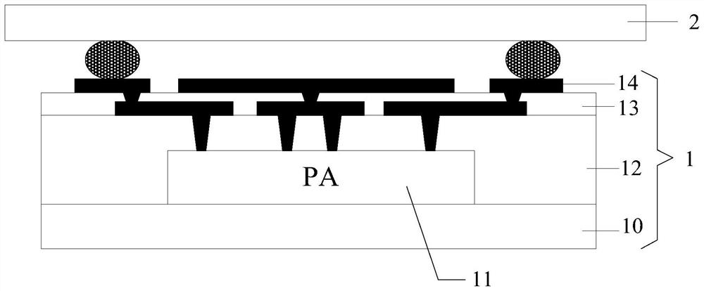
[0003] However, the current board-level architecture of the power amplifier board has the following problems: (1) the cavity height of the resonant cavity formed between the PA chip 11 and the power amplifier board 2 is low, which will cause the self-excitation problem of the power amplifier; (2) the PA chip 11 There is a problem of signal crosstalk between the RF signal on the power amplifier board 2 and the signal on the power amplifier board 2; (3) In order to reduce the signal reflection angle, it is necessary to set a ground pad on the wiring layer of the package structure 1, which will increase the occupied area of ​​the package structure 1

Method used


Image

  • Packaging module, preparation method thereof, base station and electronic equipment
  • Packaging module, preparation method thereof, base station and electronic equipment
  • Packaging module, preparation method thereof, base station and electronic equipment

Examples


Embodiment Construction

[0074] In order to make the purpose, technical solution and advantages of the application clearer, the application will be further described in detail below in conjunction with the accompanying drawings.

[0075] It should be noted that in this specification, similar numerals and letters denote similar items in the following drawings, therefore, once an item is defined in one drawing, it does not need to be identified in subsequent drawings. for further definition and explanation.

[0076] In the description of this application, it should be noted that the terms "middle", "upper", "lower", "left", "right", "vertical", "horizontal", "inner", "outer" etc. The indicated orientation or positional relationship is based on the orientation or positional relationship shown in the drawings, and is only for the convenience of describing the present application and simplifying the description, rather than indicating or implying that the referred device or element must have a specific ori...


PUM


Abstract

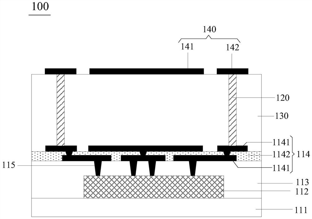
The invention discloses a packaging module, a preparation method thereof, a base station and electronic equipment. The packaging module comprises a substrate, a chip located on the substrate, a first plastic packaging layer, a wiring layer located on the plastic packaging layer, and a plurality of interconnection electrodes, a second plastic packaging layer and a conductive layer which are located on the wiring layer. The interconnection electrodes are electrically connected with the wiring layer, and the conductive layer is located on the second plastic packaging layer and comprises a grounding welding pad and a signal transmission welding pad electrically connected with the plurality of interconnection electrodes. In the packaging module, the interconnection electrodes can adjust the height of the cavity, so that the self-excitation problem of the power amplifier can be avoided. And the grounding welding pad in the conductive layer can shield the radio frequency signal on the wiring layer, so that the signal interference problem between the chip and the power amplification plate can be improved. Besides, as only the signal transmission welding pad for providing input / output signals for the chip needs to be arranged in the conducting layer, and wiring does not need to be arranged, enough area can be provided for arranging the grounding welding pad, and the occupied area of the packaging module can not be increased.

Description

technical field [0001] The present application relates to the technical field of semiconductor packaging, in particular to a packaging module, its preparation method, base station and electronic equipment. Background technique [0002] A power amplifier (Power Amplifier, PA) is an important component in a wireless communication base station. With the development of communication technology, the current 5G power amplifier multi-channel communication technology (Massive MIMO) large board is gradually evolving to a board-level architecture. The key technical point to realize the board-level architecture of the power amplifier board is that the power amplifier outputs signals from the top surface, and then interconnects the signals with the power amplifier board. A common method at present is to package the PA chip by using a flip-chip (Flip-Chip) technology. Common package structure 1 such as figure 1 As shown, the PA chip 11 is plastic-sealed on the substrate 10 through the...

Claims


Application Information

Patent Timeline
IPC IPC(8): H01L23/485H01L21/60H04W88/08
CPCH01L23/4824H01L23/485H01L24/03H01L24/83H04W88/08H01L2224/0231H01L2224/02331H01L2224/02333H01L2224/02381H01L2224/02379H01L2224/18
Inventor 郭小亚
Owner HUAWEI TECH CO LTD
Learn More