Semiconductor device

A semiconductor and conductive type technology, applied in semiconductor devices, transistors, electric solid devices, etc., can solve the problems of increased recovery current and reduced damage tolerance of diodes, and achieve the effect of improving damage tolerance

Pending Publication Date: 2022-05-31
MITSUBISHI ELECTRIC CORP
View PDF1 Cites 0 Cited by
  • Summary
  • Abstract
  • Description
  • Claims
  • Application Information

AI Technical Summary

Problems solved by technology

[0006] However, in the above-mentioned semiconductor device in which an IGBT and a diode are formed on a single semiconductor substrate, holes, which are minority carriers, flow from the IGBT region to the diode region. Compared with the case where an insulated gate bipolar transistor and a diode are connected in parallel as a separate component, there is a problem that the recovery current during the recovery operation becomes larger, and the breakdown resistance of the diode decreases.

Method used


Image

  • Semiconductor device
  • Semiconductor device
  • Semiconductor device

Examples


Embodiment approach 1

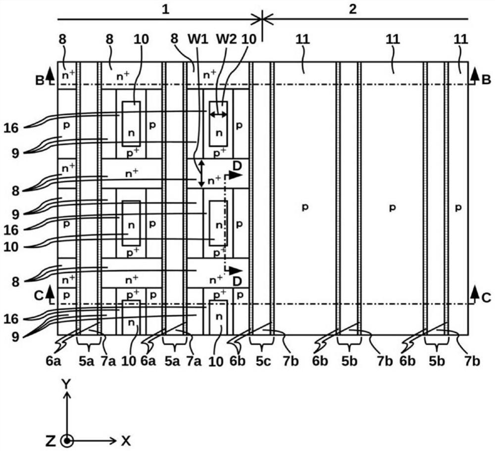
[0082] The semiconductor device according to Embodiment 1 suppresses the flow of holes h from the IGBT region 1 to the diode region 2 . Such as Figure 11 As shown, when the diode operates, holes h are injected from the p-type base layer 9 and the base contact layer 16 into the drift layer 12 of the diode region 2 . On the other hand, holes h are not injected from the n-type counter-doped layer 10 into the drift layer 12 of the diode region 2 . Therefore, by providing the anti-doped layer 10, compared with the case where the anti-doped layer 10 is not provided, the injection of holes h from the IGBT region 1 to the diode region 2 during diode operation can be suppressed. .

[0083] Therefore, by selectively providing the counter-doped layer 10 on the surface layer of the base layer 9 , the recovery current can be suppressed and the breakdown resistance at the time of the recovery operation can be improved. In addition, the concentration of the acceptor impurity in the surfa...

Embodiment approach 2

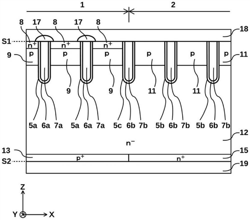
[0088] use Figure 13 and Figure 14 The structure of the semiconductor device according to Embodiment 2 will be described. Figure 13 and Figure 14 It is a plan view showing the semiconductor device according to the second embodiment. Figure 14 will be Figure 13 The enlarged view of part E described is a plan view showing the structure of the first principal surface side of the semiconductor substrate. exist Figure 14 In , the description of electrodes and the like provided on the upper side of the first main surface of the semiconductor substrate is omitted. exist Figure 13 and Figure 14 For convenience of description, XYZ orthogonal coordinate axes indicating directions are also shown in FIG. In addition, in Embodiment 2, the same constituent elements as those described in Embodiment 1 are assigned the same reference numerals and their descriptions are omitted.

[0089] Such as Figure 13 As shown, in the semiconductor device 200 according to Embodiment 2, t...


PUM


Abstract

Provided is a semiconductor device having improved breakdown tolerance during a recovery operation. An insulated gate bipolar transistor region (1) of a semiconductor device (100) is arranged in parallel with a diode region (2) in a first direction along a first main surface of a semiconductor substrate, and has: a second conductivity type base layer (9) provided on a surface layer on the first main surface side of the semiconductor substrate; an emitter layer (8) of a first conductivity type, which is selectively provided on a surface layer on the first main surface side of the base layer (9), and which has a higher impurity concentration than the drift layer; a plurality of gate electrodes (7a) arranged in parallel in the first direction and facing the emitter layer, the base layer, and the drift layer with a gate insulating film (6a) therebetween; a counter-doped layer (10) provided on the surface layer of the base layer and having a second conductivity type impurity concentration higher than that of the base layer and a first conductivity type impurity concentration higher than that of the drift layer; and a collector layer of a second conductivity type provided on a surface layer on the second main surface side of the semiconductor substrate.

Description

technical field [0001] The present invention relates to semiconductor devices. Background technique [0002] From the viewpoint of energy saving, inverter devices are widely used in fields such as home appliances, electric vehicles, and railways. Inverter devices mostly use insulated gate bipolar transistors (IGBT: [0003] Insulated Gate Bipolar Transistor) and freewheeling diodes. The insulated gate bipolar transistor and the diode are connected by wiring such as wires inside the inverter device. [0004] In order to downsize an inverter device, a semiconductor device in which an insulated gate bipolar transistor and a diode are formed on a single semiconductor substrate has been proposed (for example, Patent Document 1). [0005] Patent Document 1: Japanese Patent Laid-Open No. 2008-103590 [0006] However, in the above-mentioned semiconductor device in which an IGBT and a diode are formed on a single semiconductor substrate, holes, which are minority carriers, flow f...

Claims


Application Information

Patent Timeline
Patent Type & Authority Applications(China)
IPC IPC(8): H01L29/06H01L29/739H01L29/861H01L25/07
CPCH01L29/0638H01L29/7393H01L29/861H01L25/072H01L27/0727H01L2224/0603H01L29/0692H01L29/7397H01L29/66348H01L29/407H01L29/1095H01L29/083H01L29/0696H01L29/8613H01L29/1004H01L27/0629
Inventor 中谷贵洋新田哲也西康一
Owner MITSUBISHI ELECTRIC CORP
Why Eureka
Try Eureka