Wafer cleaning device and wafer cleaning method

A technology for cleaning devices and wafers, applied in cleaning methods and utensils, cleaning methods using liquids, chemical instruments and methods, etc., capable of solving problems such as silicon wafer surface pattern defects

Pending Publication Date: 2022-06-21
NAN YA TECH
View PDF0 Cites 0 Cited by
  • Summary
  • Abstract
  • Description
  • Claims
  • Application Information

AI Technical Summary

Problems solved by technology

However, when the protective cover is used to prevent contamination, it is also easy to cause pattern defects on the surface of the silicon wafer, especially when the crystal edge is cleaned (Bevel Rinse).

Method used


Image

  • Wafer cleaning device and wafer cleaning method
  • Wafer cleaning device and wafer cleaning method
  • Wafer cleaning device and wafer cleaning method

Examples


Embodiment Construction

[0025] Various embodiments of the present invention will be disclosed below with accompanying drawings, and for the sake of clarity, many practical details will be described together in the following description. It should be understood, however, that these practical details should not be used to limit the invention. That is, in some embodiments of the invention, these practical details are unnecessary. Besides, for the purpose of simplifying the drawings, some well-known and conventional structures and elements are shown in a simplified and schematic manner in the drawings.

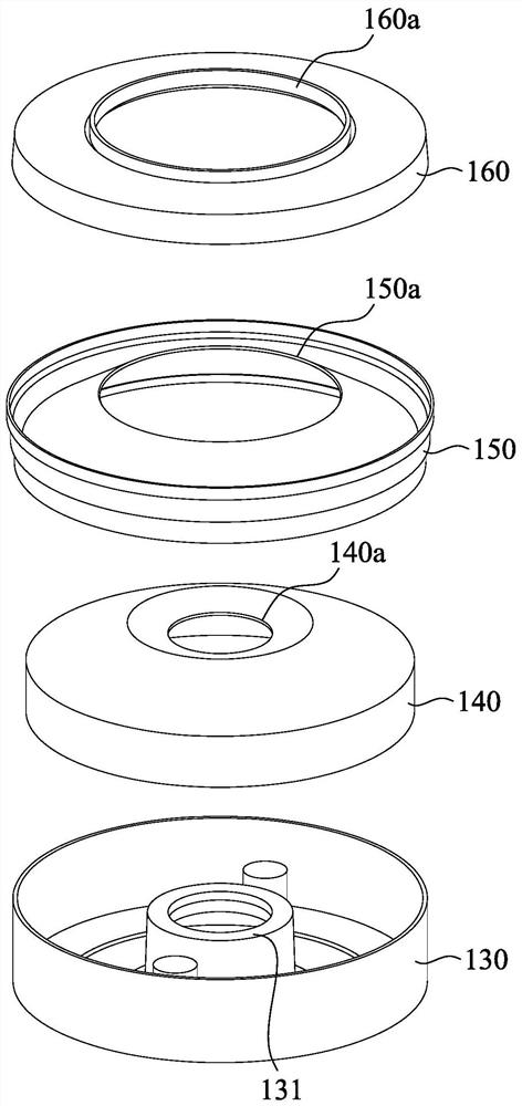
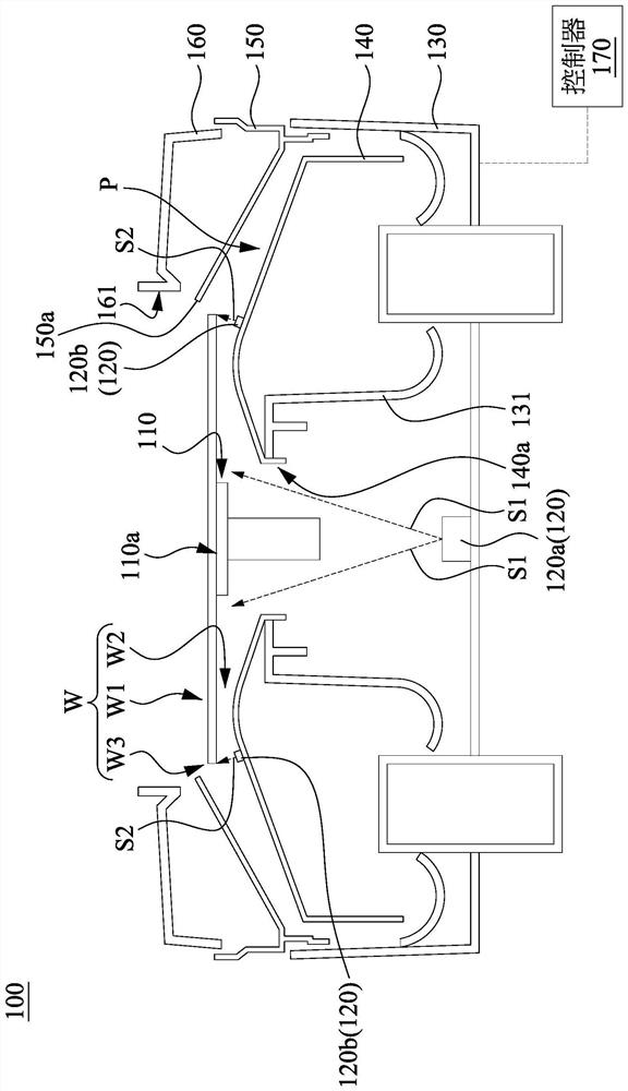
[0026] Please refer to figure 1 and figure 2 . figure 1 According to one or more embodiments of the present invention, a three-dimensional schematic diagram of some components of the wafer cleaning apparatus 100 is shown. figure 2 A schematic cross-sectional view of the wafer cleaning apparatus 100 is shown. In some embodiments of the present invention, the wafer cleaning apparatus 100 includes a ...


PUM


Abstract

The invention discloses a wafer cleaning device and a wafer cleaning method. The wafer cleaning device comprises a bearing table, at least one nozzle, a chassis, an upper shell and a lower shell. The bearing table is used for bearing a wafer, and the top surface of the wafer is coated with a photoresist. The at least one nozzle is used for spraying a cleaning solution towards the wafer. The chassis is used for recovering cleaning solution. And the lower shell is arranged on the chassis. The upper shell is arranged on the lower shell, the base plate, the lower shell and the upper shell surround and contain the bearing table, the upper shell and the lower shell jointly form a liquid flow channel extending towards the bearing table and the base plate, and the liquid flow channel is used for guiding the cleaning solution to flow to the base plate. Therefore, the wafer cleaning device can effectively spray the cleaning solution to the wafer and recover the cleaning solution.

Description

technical field [0001] The present invention relates to a cleaning device and a cleaning method, in particular to a cleaning device and method for cleaning wafers. Background technique [0002] Photoresists are widely used in the fabrication of today's integrated circuits. The photoresist is usually sprayed on the surface of the silicon wafer and shaped by the coating equipment while the silicon wafer is rotated. [0003] During the spin coating process, the sputtered photoresist is prevented from contaminating the surrounding environment by a protective cover located around the silicon wafer. However, while preventing contamination by the protective cover, pattern defects on the surface of the silicon wafer are also likely to be caused, especially during bevel rinse. [0004] Therefore, how to propose a wafer cleaning device that can solve the above problems is one of the problems that the industry is eager to solve by investing R&D resources. SUMMARY OF THE INVENTION ...

Claims


Application Information

Patent Timeline
Patent Type & Authority Applications(China)
IPC IPC(8): H01L21/67H01L21/02B08B3/02
CPCH01L21/67051H01L21/02087H01L21/0209H01L21/0206B08B3/022
Inventor 吕庚陆
Owner NAN YA TECH
Why Eureka
Try Eureka