Substrate cleaning system and substrate cleaning method

A technology for cleaning systems and substrates, which is applied in the manufacture of electrical components, circuits, semiconductors/solid-state devices, etc., and can solve problems such as corrosion

Pending Publication Date: 2022-07-01
GUANGZHOU ADVANCED SEMICON TECH CO LTD
View PDF0 Cites 0 Cited by
  • Summary
  • Abstract
  • Description
  • Claims
  • Application Information

AI Technical Summary

Problems solved by technology

For example, DICO2 / dilute-NH4OH can effectively remove static electricity, but the additive will react with Cu to cause additional corrosion

Method used


Image

  • Substrate cleaning system and substrate cleaning method
  • Substrate cleaning system and substrate cleaning method
  • Substrate cleaning system and substrate cleaning method

Examples


Embodiment Construction

[0028] In the following description, numerous specific details are set forth in order to provide a more thorough understanding of the present invention. It will be apparent, however, to one skilled in the art that the present invention may be practiced without one or more of these details. In other instances, some technical features known in the art have not been described in order to avoid obscuring the present invention.

[0029] It should be understood that when the terms "comprising" and / or "comprising" are used in this specification, they indicate the presence of said features, integers, steps, operations, elements and / or components, but do not preclude the presence or addition of one or Various other features, integers, steps, operations, elements, components and / or combinations thereof.

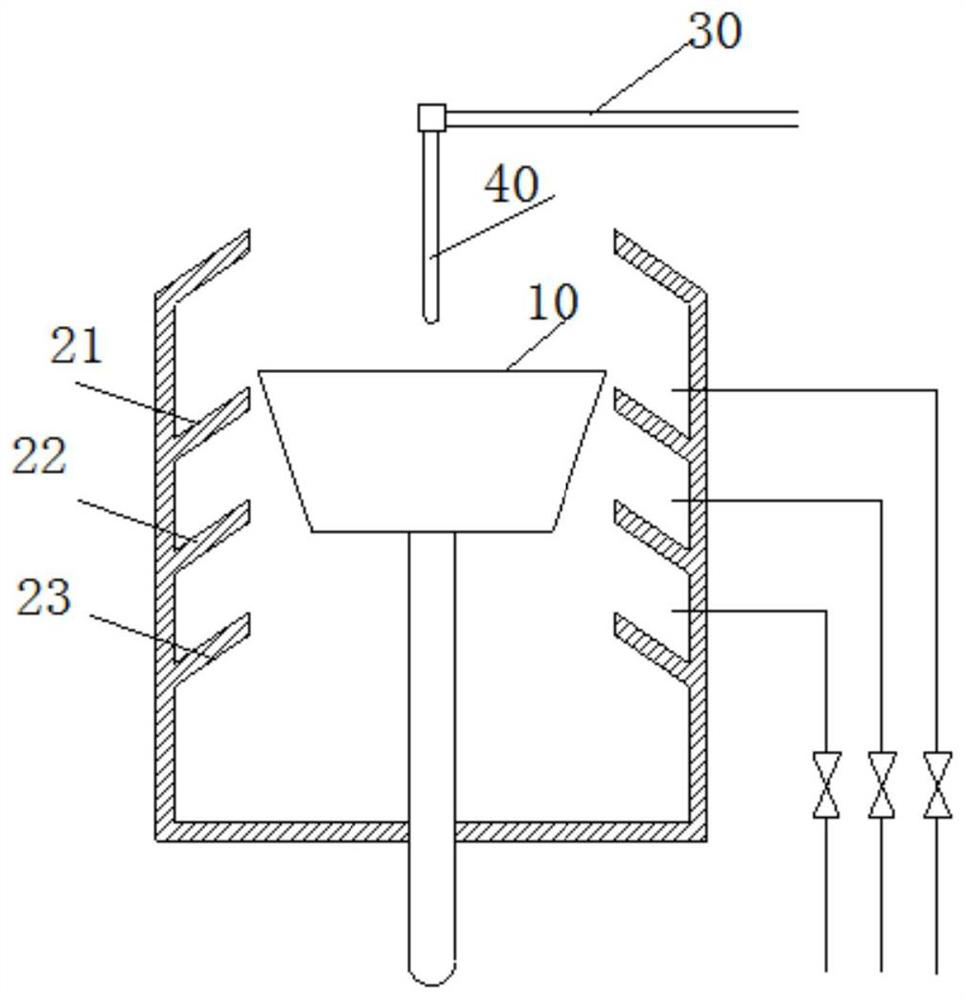
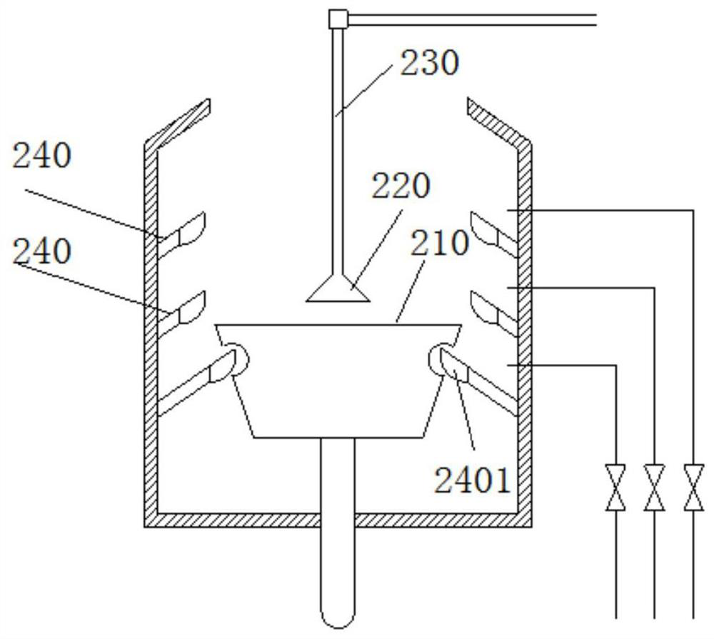
[0030] As mentioned above, the static accumulation on the surface of the DIW flowing over the wafer is related to the rotational speed of the wafer. Considering that current wet-clea...


PUM


Abstract

The invention discloses a substrate cleaning system which comprises a cavity, a supporting chuck and a spraying unit, the supporting chuck and the spraying unit are arranged in the cavity, and a substrate is fixed to the supporting chuck; the spraying unit is used for spraying washing liquid onto a substrate so as to clean the substrate, the spraying unit comprises a nozzle, and a plurality of discharge pipes arranged in an outwards inclined structure are arranged in the nozzle so that the washing liquid discharged through the discharge pipes can be uniformly sprayed onto the surface of the substrate. According to the invention, the telescopic baffle plate is used for receiving rinsed flushing fluid under the condition that the supporting chuck does not rotate, and the flushing fluid flows into the discharge layer to be treated; concentric circular holes / shower holes with different angles are designed in the nozzle so as to ensure that liquid flows through the whole substrate; when the chuck does not rotate, the liquid flow lacks an outward force, so that the nozzle arm is designed to rotate to provide an outward force for the liquid flow.

Description

technical field [0001] The present invention relates to the technical field of wafer manufacturing, and in particular, to a substrate cleaning system and a substrate cleaning method. Background technique [0002] In the processing of integrated circuits, a relatively large silicon substrate (also referred to as a wafer) undergoes many separate process steps to form a plurality of separate integrated circuits on its surface. The steps used to form these integrated circuits can be of various types, including masking, etching, deposition, diffusion, ion implantation and polishing, among many others. Typically, between the various process steps described above, the wafer must undergo a cleaning step. The cleaning step can help ensure that the integrated circuit is free from contaminants that can cause harmful defects in the delicate structure of the integrated circuit. [0003] figure 1 Shown is a schematic diagram of a typical composition of a substrate cleaning system utili...

Claims


Application Information

Patent Timeline
IPC IPC(8): H01L21/67
CPCH01L21/67051H01L21/67017
Inventor 邱奕锦孙志源林清山
Owner GUANGZHOU ADVANCED SEMICON TECH CO LTD
Why Eureka
Try Eureka