Power supply monitoring circuit and switching power supply

A technology of power monitoring and power supply voltage, applied in the direction of electrical components, output power conversion devices, etc., can solve the problems of increasing the chip area, not completely solving the problem of low voltage operation, increasing the overall power consumption of the system, and achieving small footprint, The effect of ensuring accuracy

Pending Publication Date: 2022-07-01
SG MICRO
View PDF0 Cites 0 Cited by
  • Summary
  • Abstract
  • Description
  • Claims
  • Application Information

AI Technical Summary

Problems solved by technology

For this solution, adding an external resistor R will increase the overall power consumption of the system
Increasing the width-to-length ratio of the transistor M10 and the transistor M11 in the output circuit 11 not only increases the chip area, but this circuit does not completely solve the problem of low voltage operation, and it usually requires the core circuit to be able to work at low voltage

Method used


Image

  • Power supply monitoring circuit and switching power supply
  • Power supply monitoring circuit and switching power supply
  • Power supply monitoring circuit and switching power supply

Examples


Embodiment 1

[0051] In this embodiment, the reset indication signal is valid when it is in a low level state.

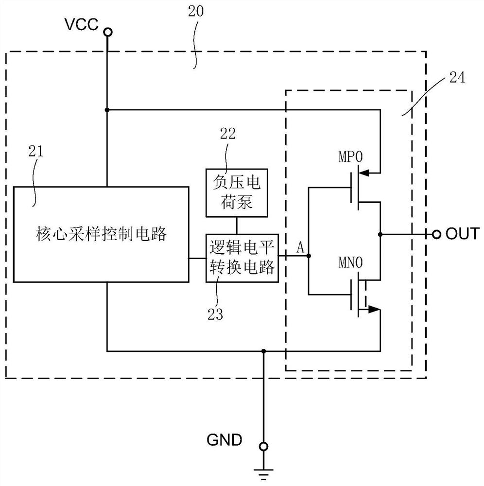
[0052] refer to image 3 , the output module 24 includes: a first switch tube MP0 and a second switch tube MN0. The first switch tube MP0 and the second switch tube MN0 are sequentially connected in series between the power supply voltage VCC input terminal and the reference ground GND, the gate of the first switch tube MP0 receives the first control signal or receives the second control signal A, and the second switch tube The gate of the transistor MN0 receives the second control signal A. Wherein, the first switch tube MP0 is an enhancement mode PMOS transistor, and the second switch tube MN0 is a depletion mode NMOS transistor. And the output module 24 outputs a reset indication signal to the output terminal OUT at the drain of the second switch tube MN0.

[0053] Further, in this embodiment, the charge pump 22 generates a reference voltage with a negative voltage VSS.

...

Embodiment 2

[0062] In this embodiment, the reset indication signal is valid when the signal is at a high level.

[0063] refer to Figure 4 , the output module 24 includes: a fourth switch tube MP1 and a fifth switch tube MN1. The fourth switch MP1 and the fifth switch MN1 are sequentially connected in series between the power supply voltage VCC input terminal and the reference ground GND, the gate of the fourth switch MP1 receives the first control signal or the second control signal A, and the fifth switch The gate of the tube MN1 receives the second control signal A. The fourth switch MP1 is a depletion-mode PMOS transistor, and the fifth switch MN1 is an enhancement-mode NMOS transistor. And the output module 24 outputs the reset indication signal to the output terminal OUT at the drain of the fourth switch tube MP1.

[0064] Further, in this embodiment, the charge pump 22 generates a reference voltage that is greater than the power supply voltage VCC.

[0065] The specific workin...

Embodiment 3

[0074] In this embodiment, the reset indication signal is valid when it is in a low level state.

[0075] refer to Figure 5 , the output module 24 includes: a first resistor R1 and a third switch tube MN2. The first resistor R1 and the third switch tube MN2 are connected in series between the power supply voltage VCC input terminal and the reference ground GND in sequence, and the gate of the third switch tube MN2 receives the second control signal A. The third switch MN2 is a depletion-mode NMOS transistor. And the output module 24 outputs a reset indication signal at the drain of the third switch tube MN2.

[0076] Further, in this embodiment, the charge pump 22 generates a reference voltage with a negative voltage VSS.

[0077] Compared with the power monitoring circuit 20 in the first embodiment, the power monitoring circuit 20 in this embodiment only replaces the PMOS transistor in the output module 24 with a resistor, and its specific working principle is basically t...


PUM


Abstract

The invention discloses a power supply monitoring circuit and a switching power supply, and the power supply monitoring circuit comprises a core sampling control module which is used for outputting a first control signal with a first logic level according to the level state of a power supply voltage; the charge pump is used for generating corresponding reference voltages according to the effective level states of different reset indication signals; the logic level conversion module is used for converting the logic level of the first control signal according to the reference voltage so as to output a second control signal with a second logic level; and the output module comprises at least one switch tube, a grid electrode receives the second control signal, the switch tube is used for outputting an effective reset indication signal at a drain electrode when the switch tube is switched on, and the switch tube is a depletion type transistor. The circuit can work normally when the power supply voltage is 0V, and is small in occupied area and high in stability and accuracy.

Description

technical field [0001] The invention relates to the technical field of power electronics, in particular to a power supply monitoring circuit and a switching power supply. Background technique [0002] For circuits such as power monitoring chips, the output pins are required to have the ability to provide a correct indication voltage even at the lowest possible power supply voltage, and to provide a sufficiently low output impedance. In order to prevent power failure, in most circuit systems, the power supply monitoring chip is used to monitor the system power supply voltage. When the power supply voltage is lower than the system operating voltage, the power supply monitoring chip outputs a logic high level or a logic low level to the core circuit. circuit reset. This requires that the power monitoring chip can provide a correct reset indication to the post-stage chip of the system under a very low power supply voltage, which requires the reset chip to work under a very low ...

Claims


Application Information

Patent Timeline
Patent Type & Authority Applications(China)
IPC IPC(8): H02M1/36H02M1/088
CPCH02M1/36H02M1/088
Inventor 王欢
Owner SG MICRO
Why Eureka
Try Eureka