Silicon carbide epitaxial growth device and growth process method

A technology of epitaxial growth and silicon carbide, applied in chemical instruments and methods, single crystal growth, single crystal growth, etc., can solve problems such as instability, difficulty in doping concentration, difficulty in meeting the requirements of high-quality MOSFET power devices, etc., and achieve reduction Edge effect, effect of uniform doping concentration

Active Publication Date: 2022-07-12
芯三代半导体科技(苏州)有限公司
View PDF13 Cites 4 Cited by
  • Summary
  • Abstract
  • Description
  • Claims
  • Application Information

AI Technical Summary

Problems solved by technology

The silicon carbide epitaxial growth process has high requirements on the uniformity of thickness and doping. Relatively speaking, it is easy to control the thickness uniformity in the process, but it is difficult to control the doping concentration.
The doping concentration uniformity of silicon carbide epitaxial wafers obtained under the current process conditions can only be 3-5%, and it is unstable, and it is difficult to meet the requirements for making high-quality MOSFET power devices.

Method used


Image

  • Silicon carbide epitaxial growth device and growth process method
  • Silicon carbide epitaxial growth device and growth process method
  • Silicon carbide epitaxial growth device and growth process method

Examples


Embodiment Construction

[0039] The above scheme will be further described below in conjunction with specific embodiments. It should be understood that these examples are intended to illustrate the present application and not to limit the scope of the present application. The implementation conditions adopted in the examples can be further adjusted such as the conditions of specific manufacturers, and the unremarked implementation conditions are usually the conditions in routine experiments.

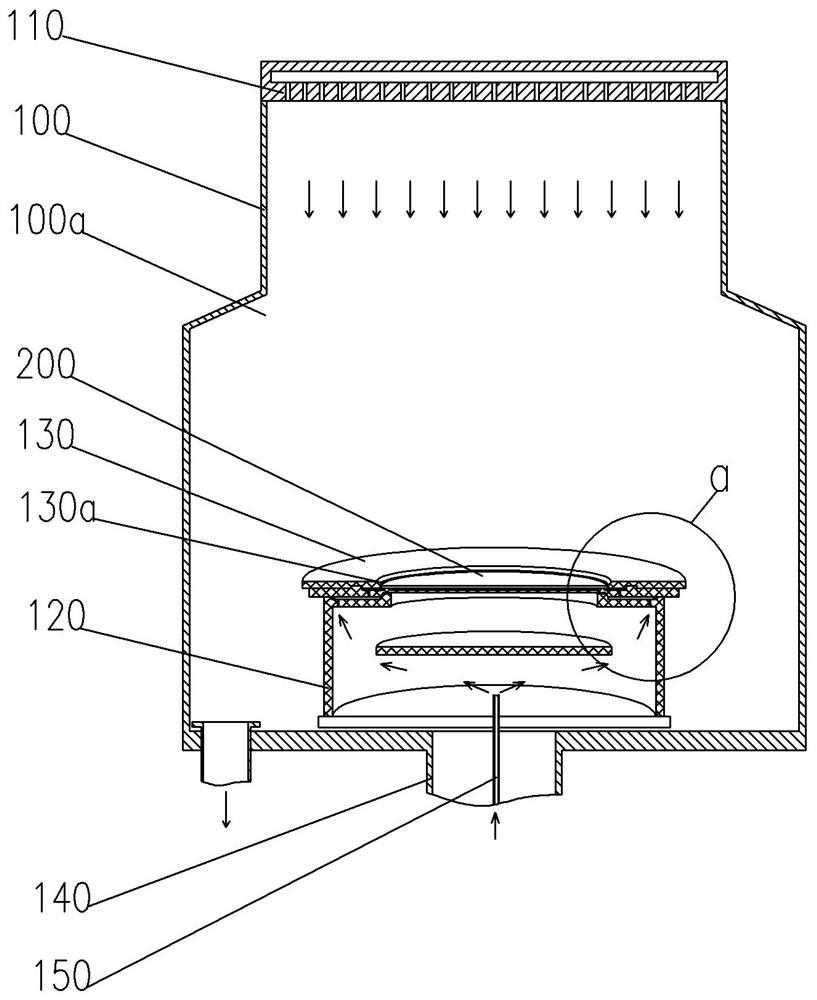
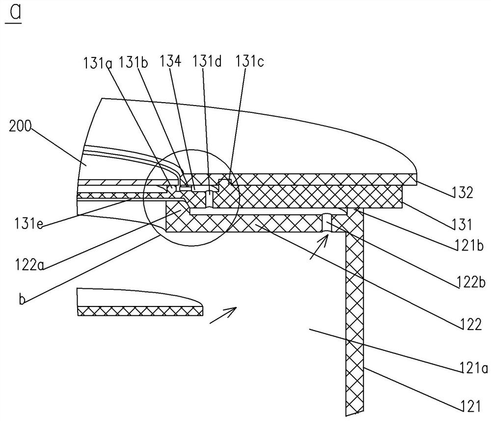
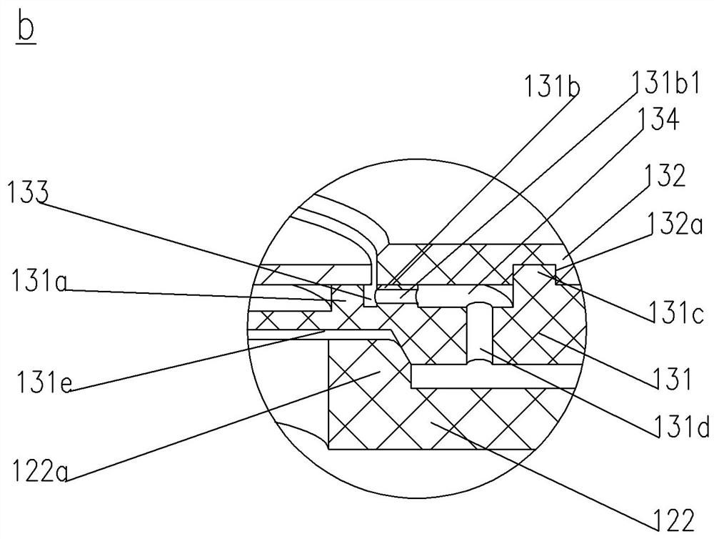
[0040] The present application provides a silicon carbide epitaxial growth device and a growth process method. The silicon carbide epitaxial growth device (hereinafter referred to as the growth device) includes: a reaction module and a rotating tray assembly, the reaction module is provided with a reaction chamber, the rotating tray assembly is arranged at the bottom of the reaction chamber, and the rotating tray assembly includes: a graphite tray and a rotating support The graphite tray is provided with a conc...


PUM

PropertyMeasurementUnit
depthaaaaaaaaaa
thicknessaaaaaaaaaa
thicknessaaaaaaaaaa

Abstract

The invention discloses a silicon carbide epitaxial growth device and a growth process method. The growth device comprises a reaction module and a rotary tray assembly, a reaction cavity is formed in the reaction module, the rotary tray assembly is arranged at the bottom of the reaction cavity, the rotary tray assembly comprises a graphite tray and a rotary supporting part, the graphite tray is provided with a concave part used for containing a substrate, an annular first groove is formed in the concave part, and the rotary supporting part is arranged in the annular first groove. The graphite tray is provided with a first groove, the first groove is configured to enable the projection of the edge of the substrate on the graphite tray to fall in the first groove, the graphite tray is provided with a plurality of edge C source gas flow paths, the edge C source gas flow paths are arranged in the circumferential direction of the first groove, and the first groove is communicated with an inner cavity of the rotary supporting part; the plurality of edge C-source gas flow paths guide the C-source gas injected into the inner cavity of the rotary support part to the first groove, and the C-source gas is guided to the edge side of the substrate through the first groove. Therefore, the C content of the edge side of the substrate is improved, the doping efficiency of the edge N is inhibited, and the purpose of uniform doping concentration is achieved.

Description

technical field [0001] The present application relates to the field of semiconductor equipment, and in particular, to a silicon carbide epitaxial growth device and a growth process method. Background technique [0002] During epitaxial growth of silicon carbide (SiC), the substrate is placed on the graphite tray in the reaction chamber of the growth device in advance, the reaction chamber is heated by a heater, and C-containing elements are introduced into the reaction chamber under appropriate conditions. And a reactive gas containing Si element to grow a SiC single crystal thin film on the substrate. Using a graphite tray to carry a substrate for epitaxial growth of silicon carbide is a common method at present, and there is no alternative. The silicon carbide epitaxial growth process has high requirements on the uniformity of thickness and doping. Relatively speaking, it is easy to control the thickness uniformity during the process, but it is difficult to control the do...

Claims


Application Information

Patent Timeline
Patent Type & Authority Applications(China)
IPC IPC(8): C30B29/36C30B25/14C30B25/12
CPCC30B29/36C30B25/14C30B25/12
Inventor 蒲勇施建新卢勇赵鹏黄名海陈清龙
Owner 芯三代半导体科技(苏州)有限公司
Why Eureka
Try Eureka