
Source-drain limited epitaxy method, device preparation method, device and equipment

A device and epitaxy technology, applied in the field of GAAFET device manufacturing process, can solve the problems of source/drain layer thickness limitation, etc., and achieve the effect of reducing stress relaxation and reducing mismatch dislocation

Pending Publication Date: 2022-07-22
FUDAN UNIV +1
View PDF0 Cites 0 Cited by
  • Summary
  • Abstract
  • Description
  • Claims
  • Application Information

AI Technical Summary

Problems solved by technology

[0008] The invention provides a source-drain limited epitaxy method, a device preparation method, and corresponding devices and equipment to solve the problem that the source / drain layer thickness between adjacent Fins of GAA devices is not limited

Method used


Image

  • Source-drain limited epitaxy method, device preparation method, device and equipment
  • Source-drain limited epitaxy method, device preparation method, device and equipment
  • Source-drain limited epitaxy method, device preparation method, device and equipment

Examples


other Embodiment approach

[0091] In other embodiments, the material for forming the first isolation layer may be other isolation materials that can achieve similar isolation effects.

[0092] In an embodiment, the forming the first isolation layer arranged along the first direction between adjacent fin structures specifically includes:

[0093] depositing an isolation layer in the plurality of source / drain cavities;

[0094] CMP processing is performed on the isolation layer; the CMP processing is a polishing process, so that the isolation layers in the plurality of source / drain cavities meet a specified height;

[0095] Photolithography and etching are performed on the isolation layer after the CMP treatment, and only the isolation layer between adjacent fin structures is retained to form the first isolation layer;

[0096] The specific steps of performing photolithography and etching on the isolation layer after the CMP treatment are: covering the surface of the device after the CMP treatment with p...

other Embodiment approach

[0110] In other embodiments, other methods may also be used to selectively etch the sacrificial layer.

[0111] 4) Filling the dummy gate cavity with a metal gate material.

[0112] Before filling the metal gate material in the dummy gate cavity, the method further includes: filling the dummy gate cavity with a high dielectric constant material; the metal gate material covers the high dielectric constant material; the high dielectric constant material Constant material and metal gate (Metalgate, MG) complete the full wrapping of the channel layer;

[0113] In one embodiment, the high dielectric constant material (High-k, HK) is a high-K material; the metal gate material is a widely used material in the prior art.

[0114] CMP processing is performed on the above-mentioned metal gate material and the high dielectric constant material, thereby removing the metal gate material and the high dielectric constant material on the top of the interlayer dielectric layer.

[0115] An e...


PUM


Abstract

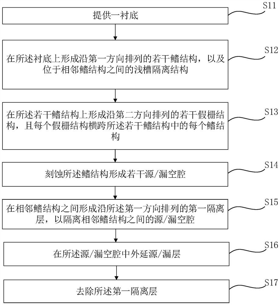
The invention provides a method for controllably limiting epitaxy of a source drain on a gate-all-around device, which comprises the following steps of: forming a plurality of fin structures arranged along a first direction on a substrate, forming a plurality of false gate structures arranged along a second direction on the plurality of fin structures, and enabling each false gate structure to stretch across each fin structure in the plurality of fin structures; etching the fin structure to form a plurality of source / drain cavities; forming a first isolation layer arranged along the first direction between the adjacent fin structures so as to isolate source / drain cavities between the adjacent fin structures; extending a source / drain layer in the source / drain cavity; and removing the first isolation layer. The thickness of the source / drain layer can be limited within the critical thickness of stress release, so that the stress relaxation phenomenon caused by mismatch and dislocation is reduced; certainly, by limiting the thickness of the source / drain layer, the area of the contact surface between the source / drain layer and the grid electrode can be limited, so that the stray capacitance is limited.

Description

technical field [0001] The invention relates to the field of GAAFET device fabrication technology, in particular to a source-drain limited epitaxy method, a device fabrication method, devices and equipment. Background technique [0002] Gate-all-around devices at advanced nodes are taller and already provide the largest active area. Stressing the channel using SiGe S / D epitaxy has been integral to device performance. [0003] The SiGe source-drain of the diamond structure exerts uneven stress on the channels of nanowires or nanosheets at different stacking levels, and it is difficult to control uniformity. [0004] In gate-all-around devices, the device current is improved by increasing the number of stacked nanowires or nanosheets, and the height of the fin structure (Fin) increases with the increase of the number of stacked nanowires or nanosheets. [0005] As the height of Fin increases, the volume of epitaxial SiGe increases, and the SiGe source and drain between singl...

Claims


Application Information

Patent Timeline
IPC IPC(8): H01L21/336H01L29/06H01L29/08H01L29/78
CPCH01L29/785H01L29/66795H01L29/0642H01L29/0847
Inventor 刘桃徐敏张卫汪大伟孙新陈鲲杨静雯吴春蕾王晨徐赛生尹睿
Owner FUDAN UNIV
Learn More