Multimode Kerr optical frequency comb generation device based on two-dimensional material nanobelt
A technology of two-dimensional materials and nanoribbons, applied in optical components, instruments, optics, etc., can solve problems such as regulating Kerr optical frequency combs, achieve the effect of lowering the threshold, reducing costs, and realizing mass production
- Summary
- Abstract
- Description
- Claims
- Application Information
AI Technical Summary
Problems solved by technology
Method used
Image


Examples
Embodiment 1
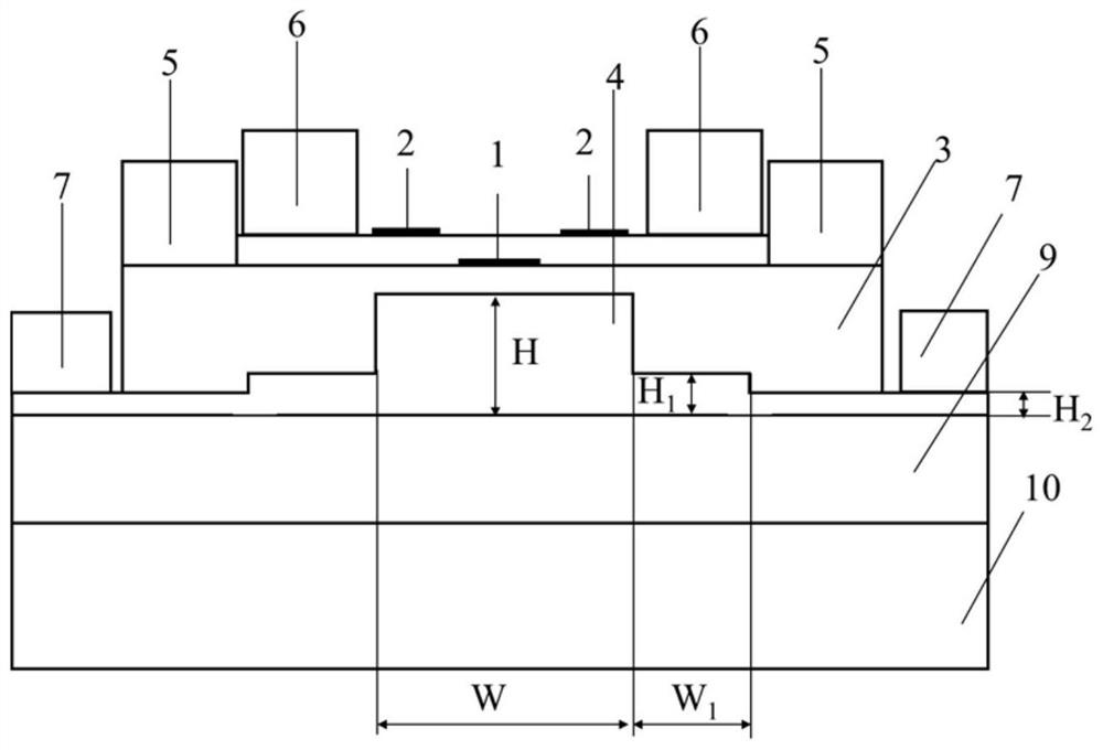
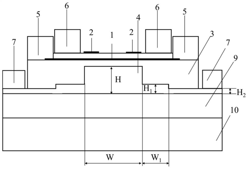
[0044] As shown in Figure 2(a), the waveguide material is selected as silicon material, the insulating cladding material is selected as alumina material, the width W of the waveguide layer in the multimode micro-resonator is 600 nm, the width W1 of the plate 1 is 300 nm, and the waveguide layer is 300 nm. The layer thickness H is 500 nm, the thickness H1 of the plate 1 is 150 nm, the thickness H2 of the plate 2 is 70 nm, the two-dimensional material nanoribbons are set to graphene, the graphene width of the first layer of two-dimensional material nanoribbons 1 is set to 200 nm, and the second layer The graphene width of the two-dimensional material nanoribbon 2 is set to 120 nm, and the TE in the multi-mode micro-resonator 4 is calculated. 0 , TE 1 The dispersion curve of the mode is as image 3 shown. The Fermi levels of the first layer of 2D material nanoribbons 1 and the second layer of 2D material nanoribbons 2 are set to 1.0 eV and 0.4 eV, respectively, corresponding to...
Embodiment 2
[0051] As shown in Figure 2(a), the waveguide material is selected as silicon material, and the insulating cladding material is selected as alumina material. The layer thickness H is 500 nm, the thickness H1 of the plate 1 is 150 nm, the thickness H2 of the plate 2 is 70 nm, the two-dimensional material nanoribbons are set to graphene, the graphene width of the first layer of two-dimensional material nanoribbons 1 is set to 200 nm, and the second layer The graphene width of the two-dimensional material nanoribbon 2 is set to 120 nm, and the TE in the multi-mode micro-resonator is calculated. 0 , TE 1 The dispersion curve of the mode is as image 3 shown. The Fermi levels of the first layer of 2D material nanoribbons 1 and the second layer of 2D material nanoribbons 2 are set to 0.5 eV and 1.0 eV, respectively, corresponding to TE 0 and TE 1 The waveguide optical losses of the modes are 2.1*10 -4 μm -1 and 4.4*10 -5 μm -1 . The spectral output of the dual-mode Kerr opt...
PUM
 Abstract
Description
Claims
Application Information
 - R&D
- Intellectual Property
- Life Sciences
- Materials
- Tech Scout
- Unparalleled Data Quality
- Higher Quality Content
- 60% Fewer Hallucinations
Browse by: Latest US Patents, China's latest patents, Technical Efficacy Thesaurus, Application Domain, Technology Topic, Popular Technical Reports.
© 2025 PatSnap. All rights reserved.Legal|Privacy policy|Modern Slavery Act Transparency Statement|Sitemap|About US| Contact US: help@patsnap.com