Production process of micro-display

A production process and micro-display technology, applied in the field of micro-display, can solve the problems of affecting product appearance, affecting wire bonding, and easy overflow of glue, etc., to achieve the effect of improving display abnormalities and reducing edge differences

Pending Publication Date: 2022-07-29
ANHUI SEMICON INTEGRATED DISPLAY TECH CO LTD
View PDF0 Cites 0 Cited by
  • Summary
  • Abstract
  • Description
  • Claims
  • Application Information

AI Technical Summary

Problems solved by technology

[0005] 3. After glue dispensing of the module, because the outer edge of the pixel area is lower, the glue flows away quickly, and the glue on the edge is thinner. After the glass cover is attached, the glue is easy to overflow under the action of glass and pressing, and overflows to the PAD affects wire bonding, or affects product appearance

Method used


Image

  • Production process of micro-display
  • Production process of micro-display
  • Production process of micro-display

Examples


Embodiment Construction

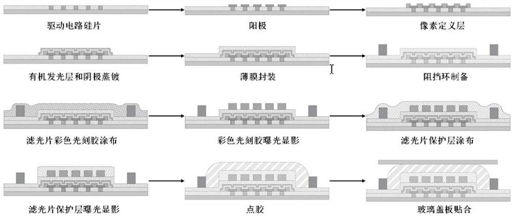
[0032] Below with reference to the accompanying drawings, through the description of the embodiments, the specific embodiments of the present invention will be described in further detail, the purpose is to help those skilled in the art to have a more complete, accurate and in-depth understanding of the concept and technical solutions of the present invention, and contribute to its implementation.

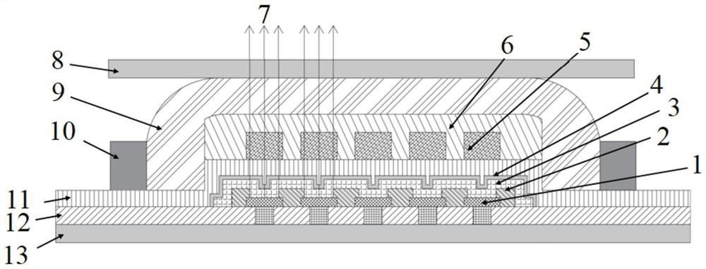
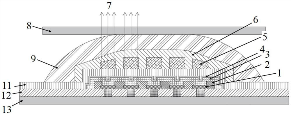
[0033] like figure 1 and figure 2 As shown, the present invention provides a production process of a microdisplay, comprising the steps of:

[0034] S1. Prepare a drive circuit on a silicon wafer;

[0035] S2, prepare the anode layer;

[0036] S3, prepare a pixel definition layer;

[0037] S4, vapor deposition organic light-emitting layer and cathode layer;

[0038] S5, thin film packaging;

[0039] S6, prepare a circle of blocking rings outside the pixel area;

[0040] S7, coating the color photoresist, and the blocking ring prevents the spin-coated color photoresist from...


PUM


Abstract

The invention discloses a production process of a micro-display. The production process comprises the following steps: S1, preparing a driving circuit on a silicon wafer; s2, preparing an anode layer; s3, preparing a pixel definition layer; s4, evaporating an organic light-emitting layer and a cathode layer; s5, thin film packaging; s6, preparing a circle of blocking ring outside the pixel region; s7, coating the color photoresist, and preventing the spin-coated color photoresist from being thrown away by a blocking ring; s8, exposing and developing the color photoresist, wherein the blocking ring can inhibit the edge from being excessively washed by developing liquid and water; s9, coating a protective layer of the optical filter; s10, the optical filter protection layer is exposed and developed, a blocking ring prevents color photoresist of the optical filter protection layer from overflowing, and the film thickness of the protection layer is guaranteed; s11, dispensing the glue on the module, preventing the glue from flowing away by a blocking ring, and ensuring the thickness of the glue on the edge of the pixel region; and S12, laminating the glass cover plate. According to the production process of the micro-display, the edge difference of the pixel region can be reduced, and the display abnormity can be improved.

Description

technical field [0001] The invention belongs to the technical field of microdisplays, and in particular, the present invention relates to a production process of a microdisplay. Background technique [0002] Microscopic technology has been widely used in near-eye display terminal products, including virtual reality (VR), augmented reality (AR), mixed reality (MR), etc. Compared with conventional low-resolution displays such as mobile phones, TVs, and computers, the size of microdisplays is small, and the display abnormalities caused by edge effects are more obvious. Near-eye display systems generally use complex optical systems to magnify images to enhance immersion, which will further magnify display abnormalities. For example, VR uses lenses and Fresnel lenses; AR and MR use transflective projection display technology. The display is transmitted through optical waveguides and enlarged by magnifying gratings, and finally presents graphics to the human eye. like image 3 As...

Claims


Application Information

Patent Timeline
IPC IPC(8): H01L27/32
CPCH10K59/38H10K59/124H10K59/122H10K59/1201
Inventor 吕迅刘胜芳刘晓佳陆瑞王澳颜强盖
Owner ANHUI SEMICON INTEGRATED DISPLAY TECH CO LTD
Why Eureka
Try Eureka