Spatial light modulator and design method and light beam scanning method thereof
A spatial light modulator and beam scanning technology, applied in instruments, optics, optical components, etc., can solve the problems of high power consumption, slow response speed of devices, and small changes in the refractive index of materials, and achieve simple structure, improve modulation depth, Effects of low-phase-shift cell structure
- Summary
- Abstract
- Description
- Claims
- Application Information
AI Technical Summary
Problems solved by technology
Method used
Image
Examples
Embodiment 1
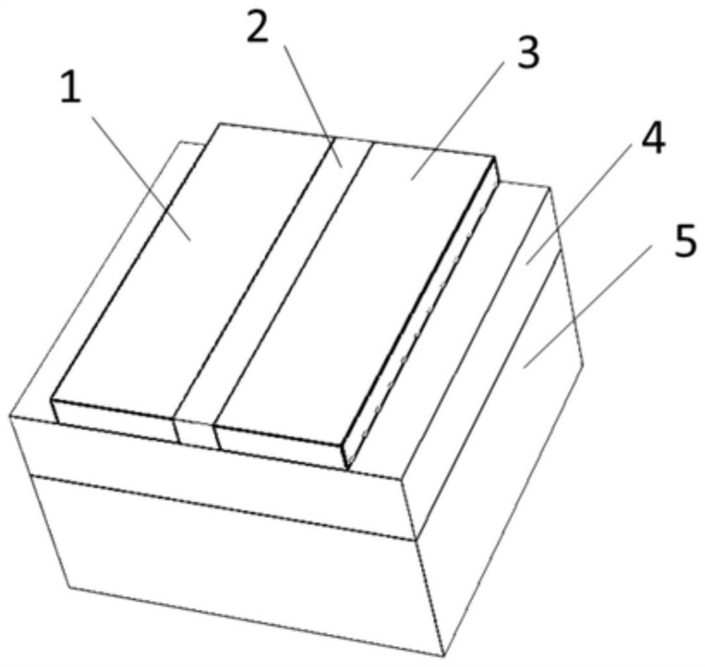
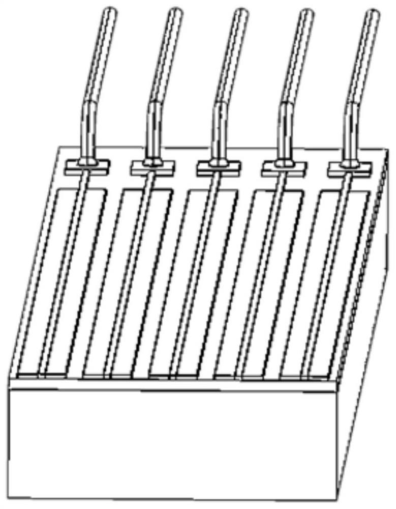
[0049] As an embodiment, the embodiment of the present invention can provide an all-solid-state nano-spatial light modulator, the technical idea is to electrically drive the vanadium dioxide material to generate a reflective array composed of nano-resonators with continuously changing phases. In a specific implementation process, an electrically tunable plasmonic nano-resonator unit is provided, specifically a top layer, a middle layer and a bottom layer. The top layer is a nano-antenna, the middle layer is an aluminum oxide insulating film, and the bottom layer is an aluminum mirror substrate. The top nanoantenna adopts a vanadium dioxide-gold-vanadium dioxide structure and is symmetrical in the middle. like figure 1 As shown, in a specific embodiment, the first vanadium dioxide structure 1 , the gold electrode 2 , and the second vanadium dioxide structure 3 may be arranged in order from left to right. The middle layer is an aluminum oxide layer 4 , and the bottom layer is ...
Embodiment 2
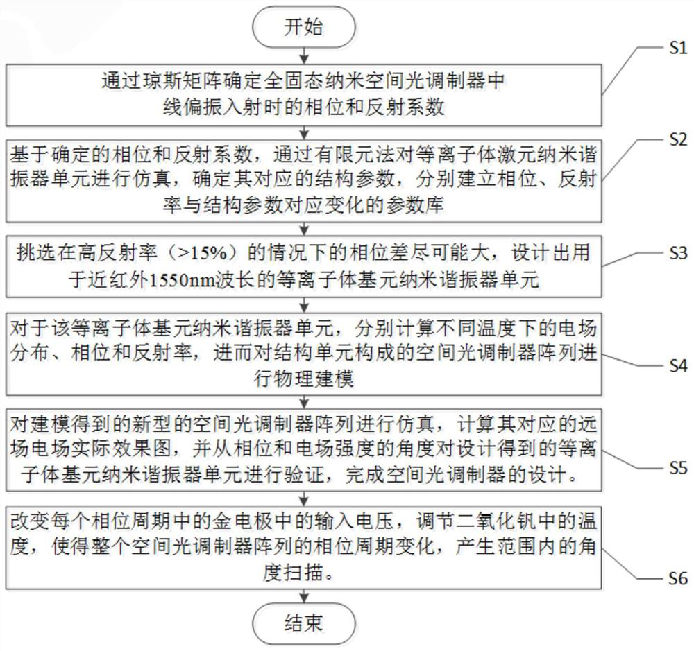
[0055] As an implementation, as image 3 As shown, an embodiment of the present invention provides a method for designing an all-solid-state nano-spatial light modulator, including the following steps:
[0056] S1. Determine the phase and reflection coefficient of the all-solid-state nano-spatial light modulator when linearly polarized by the Jones matrix;
[0057] S2. Based on the determined phase and reflection coefficient, considering the influence of the vanadium dioxide phase transition on the optical properties of the structure, use the optical parameters before and after the phase transition to simulate the plasmonic nano-resonator unit by the finite element method, and determine For the corresponding structural parameters, establish a parameter library with corresponding changes in phase, reflectivity and structural parameters, such as Figure 5 shown;
[0058] S3. Compare and analyze the reflectivity and phase of the plasmonic nano-resonator unit before and after th...
Embodiment 3
[0069] As an implementation, as Figure 4 As shown, an embodiment of the present invention provides a beam scanning method for an all-solid-state nano-spatial light modulator, including the following steps:
[0070] SS1. Establish the phase-reflectivity spectrum of the model structure at different temperatures by simulating the plasmonic nano-resonator unit in detail;
[0071] SS2. Take five adjacent plasmonic nano-resonators as a phase cycle, assign a corresponding phase to each phase cycle according to different phase gradients, and adjust to the corresponding temperature according to the phase-reflectivity spectrum;
[0072] SS3. Different phase gradients will produce different reflection angles, and gradually adjust the phase gradient of the phase cycle to form an angular scan of the reflected beam.
[0073] Among them, the deflection angle of the reflected light is determined according to the generalized Snell formula of the metasurface.
[0074] In step SS3, when desig...
PUM
| Property | Measurement | Unit |
|---|---|---|
| Width | aaaaa | aaaaa |
Abstract
Description
Claims
Application Information


