Method for quickly and freely depositing or etching atomic layer and chamber structure

An atomic layer and chamber technology, applied in the field of method and chamber structure, fast and free deposition or etching of atomic layer, can solve the problems of slow growth or etching material rate, mutual contamination of precursor sources, etc., to improve deposition or Etching rate, avoiding cross-contamination, and improving work efficiency

Pending Publication Date: 2022-08-05
江苏鹏举半导体设备技术有限公司
View PDF0 Cites 1 Cited by
  • Summary
  • Abstract
  • Description
  • Claims
  • Application Information

AI Technical Summary

Problems solved by technology

[0003] However, in the prior art, the deposition or etching reaction is often carried out in one reaction chamber, and the gas pipeline also uses the same pipeline, which can easily lead to mutual contamination of different precursor sources, and the input, discharge, blowing of precursor sources Scanning is done in the same chamber, resulting in slow growth or etching material

Method used


Image

  • Method for quickly and freely depositing or etching atomic layer and chamber structure
  • Method for quickly and freely depositing or etching atomic layer and chamber structure
  • Method for quickly and freely depositing or etching atomic layer and chamber structure

Examples


Embodiment Construction

[0036] In order to deepen the understanding of the present invention, the present invention will be described in further detail below with reference to the examples. The following examples are only used to explain the present invention and do not constitute a limitation on the protection scope of the present invention.

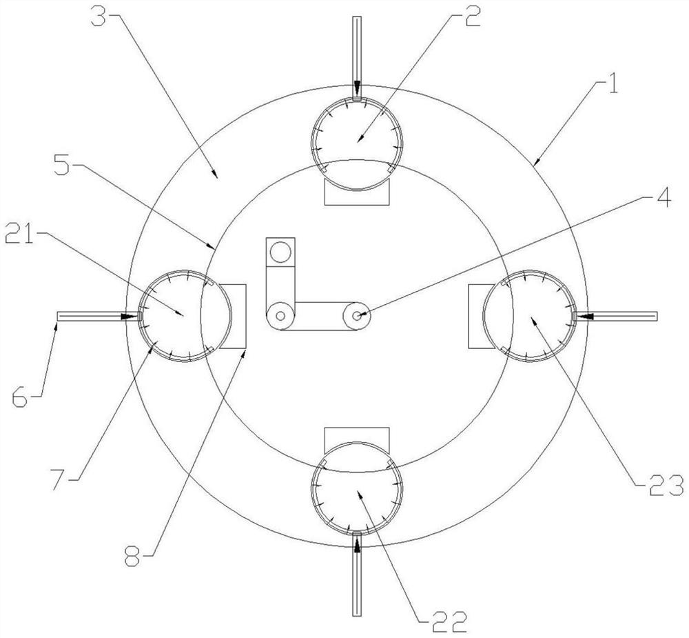
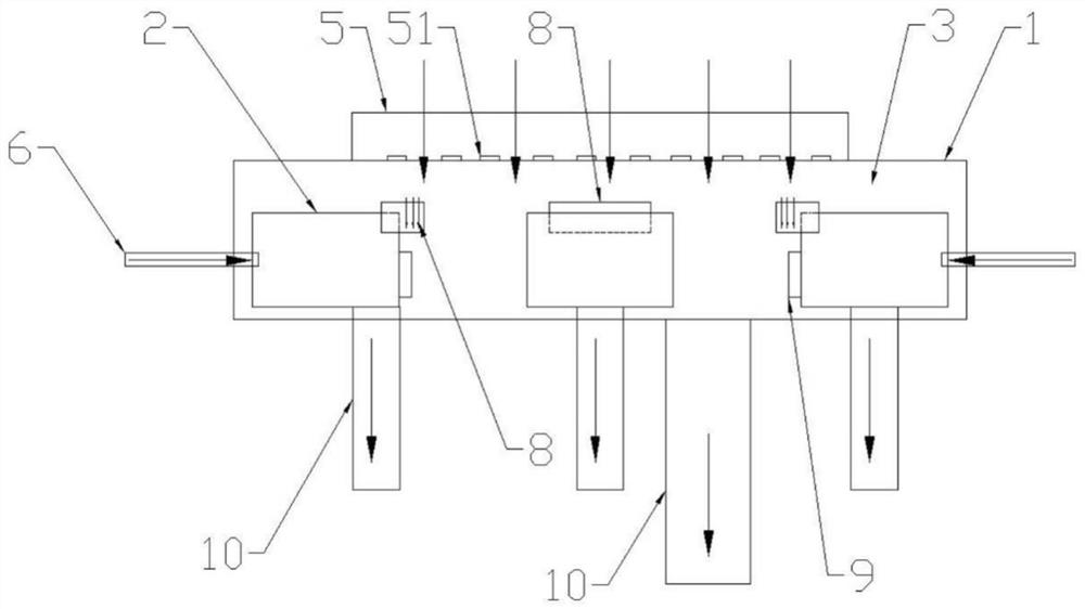
[0037] like Figure 1-6 As shown, a chamber structure for rapidly and freely depositing or etching atomic layers includes a disk chamber 1, and the disk chamber 1 is provided with a number of source reaction chambers 2 arranged in a circular ring. Chamber 2 provides the reaction place for the entire process, and each source reaction chamber 2 has only a single precursor source influx, which is carried by the carrier gas to avoid cross-infection of different precursor sources. The source reaction chamber 2 is outside the transmission chamber. 3;

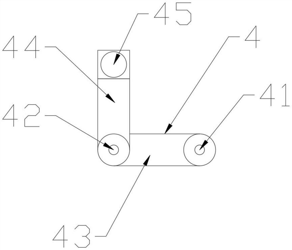
[0038] The middle of the disk chamber 1 is provided with at least one substrate transmission device 4 that rotates...


PUM


Abstract

The invention belongs to the technical field of atomic layers, and provides a method for quickly and freely depositing or etching an atomic layer and a chamber construction.The chamber structure comprises a disc chamber, a plurality of source reaction chambers which are annularly arranged at equal intervals are arranged in the disc chamber, and transmission chambers are arranged outside the source reaction chambers; at least one substrate transmission device rotating around the circle center of the disc cavity is arranged in the middle of the disc cavity; according to the invention, the deposition or etching reaction is carried out through the rotary reciprocating motion of the substrate carrying transmission device, the deposition or etching rate is improved while the deposition or etching effect is ensured, and the deposition or etching efficiency can be improved by setting different cavity numbers and operation programs according to the types of deposition or etching materials. And automatic and intelligent deposition or etching of various materials is realized.

Description

technical field [0001] The invention belongs to the technical field of atomic layers, and in particular relates to a method for depositing or etching atomic layers quickly and freely and a chamber structure. Background technique [0002] ALD (Atomic layer deposition) is a method in which gas-phase precursors are alternately passed into the reactor, chemically adsorbed on the deposition substrate and reacted to form a deposited film. A method of layer-by-layer plating on the surface of a substrate, ALD is a true nanotechnology that achieves nano-scale ultra-thin film deposition in a precisely controlled manner. Since ALD utilizes the characteristics of saturated chemical adsorption, it can ensure that large High conformal uniform deposition of area, porous, tubular, powder or other complex-shaped substrates Remove material. [0003] However, in the prior art, deposition or etching reactions are often carried out in one reaction chamber, and the same gas pipeline is also use...

Claims


Application Information

Patent Timeline
Patent Type & Authority Applications(China)
IPC IPC(8): H01J37/32H01L21/316H01L21/311H01L21/67H01L21/677
CPCH01J37/32899H01J37/32449H01L21/67213H01L21/67069H01L21/67706H01L21/67742H01L21/31122H01L21/02178H01L21/0228H01J2237/3321H01J2237/3341
Inventor 刘磊唐继远张洪国张海飞李正磊房岩王浩增徐道涵卓永生
Owner 江苏鹏举半导体设备技术有限公司
Why Eureka
Try Eureka