
Eureka
For R&D, Eureka makes reading and utilizing patents & technical documents easy.
Eureka AIR
Designed for self-driven R&D workflows. Generate viable solutions, solve complex R&D challenges, empower your innovation with AI.

Eureka Materials
Designed for material experts only. Revolutionize your material R&D, from search, analyze, to developing new materials.

TechResearch
Generate reliable direction feasibility study reports for your R&D in just a few steps.

TechSeek
Discover and master advanced knowledge NOW. Basics, ideas, possibilities, all at once.

TechMind
As an expert in R&D Theories, TechMind can generates customized viable solutions instantly.

TechRisk
Analyze your overall solution with one click, know your potential R&D risks in advance.

TechMonitor
Get weekly tech updates, stay abreast of the latest tech innovations and key insights.
Low-on-resistance SGT preparation method, semiconductor device and equipment
A low on-resistance, conductive plug technology, applied in the direction of semiconductor devices, semiconductor/solid-state device manufacturing, semiconductor/solid-state device components, etc. Difficult to eliminate, main on-resistance reduction effect
- Summary
- Abstract
- Description
- Claims
- Application Information
AI Technical Summary
Problems solved by technology
Method used
Image

Examples
preparation example Construction
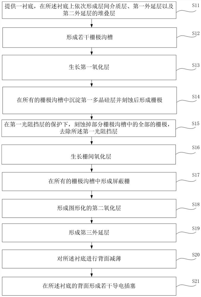
[0064] The preparation technology of prior art SGT product is:
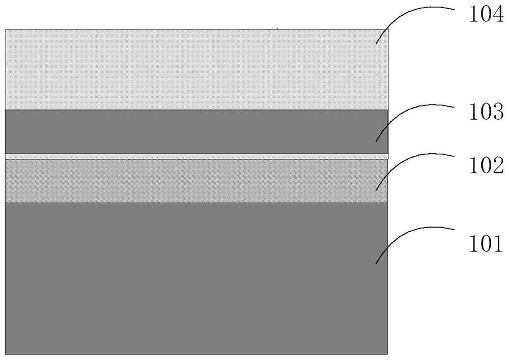
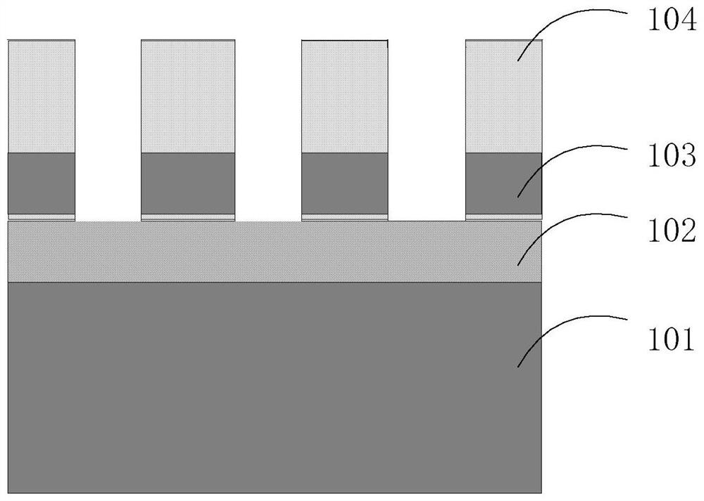
[0065] growing an epitaxial layer on a substrate;
[0066] A hard mask layer and a photoresist are sequentially deposited on the substrate, the photoresist is patterned, and the hard mask layer is etched using the patterned photoresist as a mask to form a patterned hard mask layer for patterning The hard mask layer is a mask to etch the epitaxial layer, remove the photoresist, and form a gate trench;
[0067] growing an oxide layer on the surface of the substrate and in the gate trench, and then forming a shielding gate, an oxide layer between gates and a gate in the gate trench in sequence;
[0068] Implanting P-type ions and N-type ions in the epitaxial layer around the gate to form source and well regions;
[0069] Deposit an interlayer dielectric layer on the surface of the epitaxial layer and the top of the gate, coat photoresist on the surface of the interlayer dielectric layer, pattern the photoresist, a...
PUM
 Abstract
Description
Claims
Application Information
 - R&D Engineer
- R&D Manager
- IP Professional
- Industry Leading Data Capabilities
- Powerful AI technology
- Patent DNA Extraction
Browse by: Latest US Patents, China's latest patents, Technical Efficacy Thesaurus, Application Domain, Technology Topic, Popular Technical Reports.
© 2024 PatSnap. All rights reserved.Legal|Privacy policy|Modern Slavery Act Transparency Statement|Sitemap|About US| Contact US: help@patsnap.com