Wiring structure and method for wafer substrate standard integration area suitable for on-chip integration

A technology of wiring structure and integration area, applied in the direction of semiconductor/solid-state device components, semiconductor devices, electrical components, etc., can solve the problems of non-guarantee and high yield, and achieve the effect of improving compatibility and improving production yield

Active Publication Date: 2022-08-05
ZHEJIANG LAB
View PDF11 Cites 0 Cited by
  • Summary
  • Abstract
  • Description
  • Claims
  • Application Information

AI Technical Summary

Problems solved by technology

Secondly, despite controlling the size of the photomask, under the condition of too many metal layers, a high yield cannot be guaranteed
Studies

Method used


Image

  • Wiring structure and method for wafer substrate standard integration area suitable for on-chip integration
  • Wiring structure and method for wafer substrate standard integration area suitable for on-chip integration
  • Wiring structure and method for wafer substrate standard integration area suitable for on-chip integration

Examples


Example Embodiment

[0046] The specific embodiments of the present invention will be described in detail below with reference to the accompanying drawings. It should be understood that the specific embodiments described herein are only used to illustrate and explain the present invention, but not to limit the present invention.

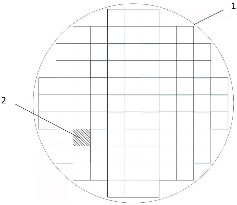
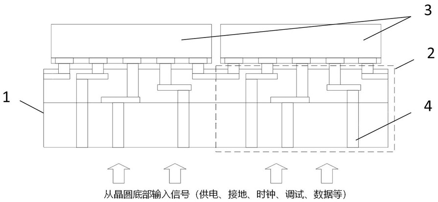
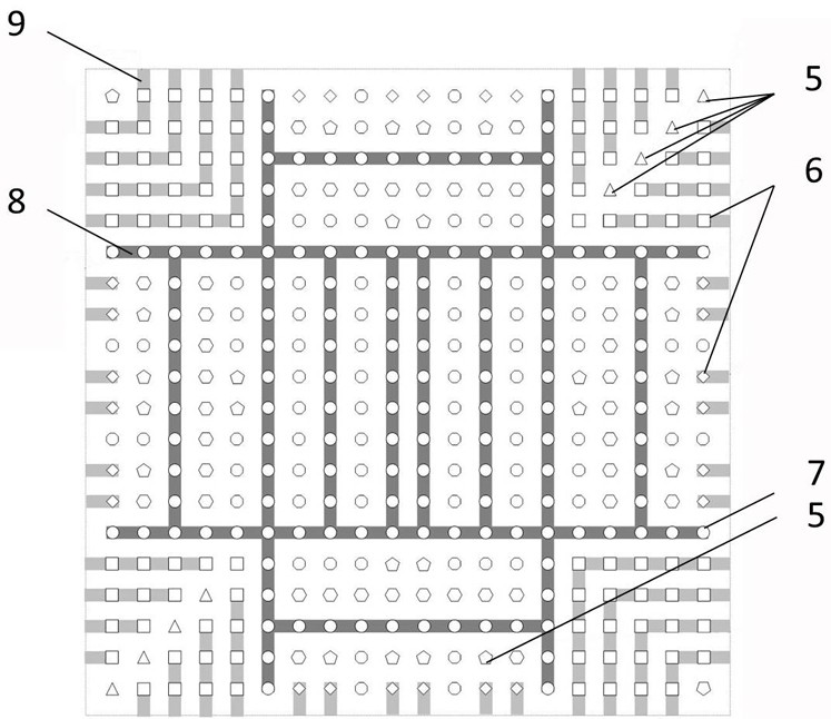
[0047]Wafer substrate standard integrated area wiring structure suitable for on-chip integration, such as figure 1 , figure 2 As shown, an area is divided on the wafer substrate 1 as a standard integrated area 2. The standard integrated area 2 is provided with pins upward, and an on-chip wiring network is constructed by connecting the pins. Each standard integrated area includes three metal layers, such as Figure 3 to Figure 5 As shown, the top metal layer includes core voltage pins 7, interconnection signal pins 6 and complex function pins 5, the middle metal layer includes clock signal pins 10, and the bottom metal layer includes ground pins 12;

[0048] Connect th...


PUM


Abstract

The invention discloses a wafer substrate standard integration area wiring structure and method suitable for on-chip integration, the wafer substrate standard integration area wiring structure comprises a core voltage network, an interconnection signal network, a clock signal network and a ground wire network, the core voltage network and the interconnection signal network belong to a top metal layer, the clock signal network is located in a middle metal layer, and the ground wire network is located in the middle metal layer. The ground wire network is located on the bottom metal layer. Pins provided upwards by the standard integration area comprise a core voltage pin, an interconnection signal pin, a clock signal pin, a ground wire pin and a complex function pin, the complex function pin is directly connected to the outside of the system through a TSV at the bottom of a wafer, and the other pins are connected through a signal network to which the pins belong; the core voltage pins and the ground wire pins are distributed in a centrosymmetric #-shaped core voltage area in a stripe staggering mode, and the interconnection signal pins are distributed in an interconnection signal area around a standard integration area. According to the invention, the problem of low yield of metal wiring of the wafer substrate caused by a large number of wiring layers and lack of wiring planning is solved.

Description

technical field [0001] The present invention relates to the technical fields of micro-nano processing, redistribution layer (RDL) and on-chip integration, in particular to a wafer substrate standard integrated area wiring structure and method suitable for on-chip integration. Background technique [0002] With the gradual failure of Moore's Law and Dennard's Law of Scaling, the improvement of computing performance by technological progress has slowed down significantly, while the amount of data in the Internet of Everything has exploded exponentially, and the "scissors" gap between data scale and computing power is getting wider and wider. The larger the integrated circuit, the period of major technological and industrial changes in the "post-Moore era" is coming. [0003] In view of the unsustainable problem of Moore's Law, the System on Wafer (SOW) has attracted the attention of academia and industry, and used it to expand Moore's Law. Its main connotation is to directly ...

Claims


Application Information

Patent Timeline
IPC IPC(8): H01L23/485H01L23/48H01L23/528H01L21/768H01L21/60
CPCH01L23/4824H01L23/485H01L23/481H01L23/5286H01L24/03H01L21/76898H01L2224/0231H01L2224/02331H01L2224/02381H01L2224/02379H01L2224/02375
Inventor 李顺斌王伟豪张汝云刘勤让万智泉沈剑良
Owner ZHEJIANG LAB
Why Eureka
Try Eureka